

CMOS-compatible silicon nano-wire sensors with biochemical and cellular interfaces
a biochemical and cellular interface technology, applied in nanoinformatics, instruments, biochemical apparatus and processes, etc., can solve the problems of poor sensing capability, poor material and device service life of typical silicon-based nano-wire fabrication processes, and unreliable product performance and consistency, so as to improve sensitivity and large surface to volume ratio
- Summary
- Abstract
- Description
- Claims
- Application Information
AI Technical Summary
Benefits of technology
Problems solved by technology
Method used
Image

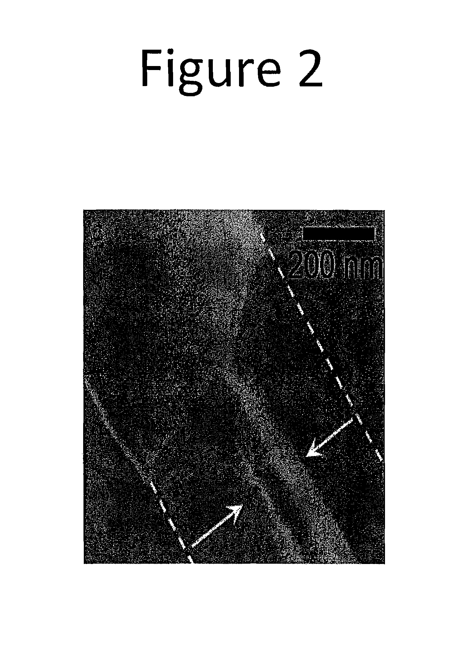
Examples
Embodiment Construction
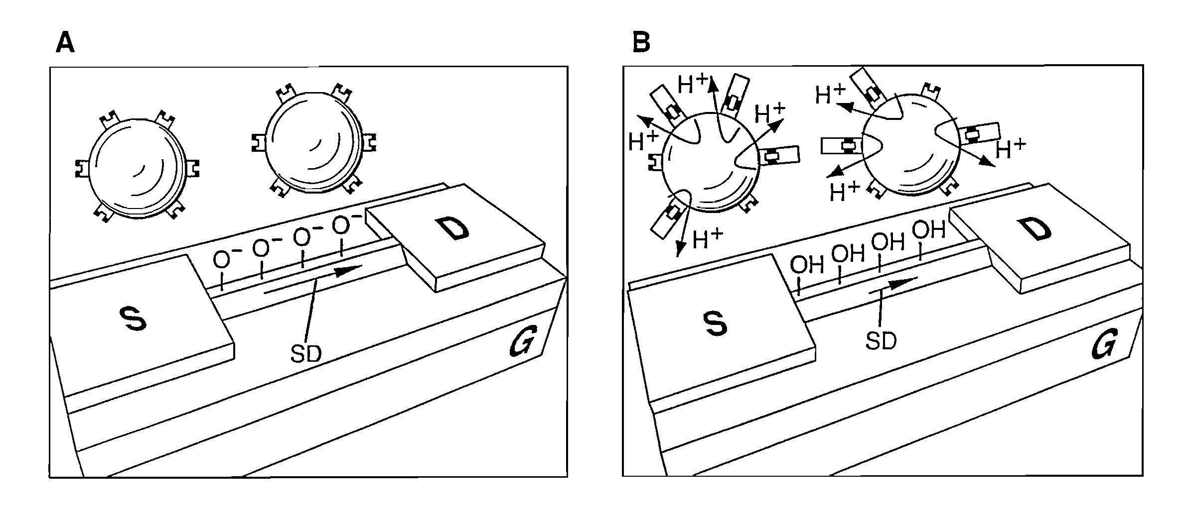
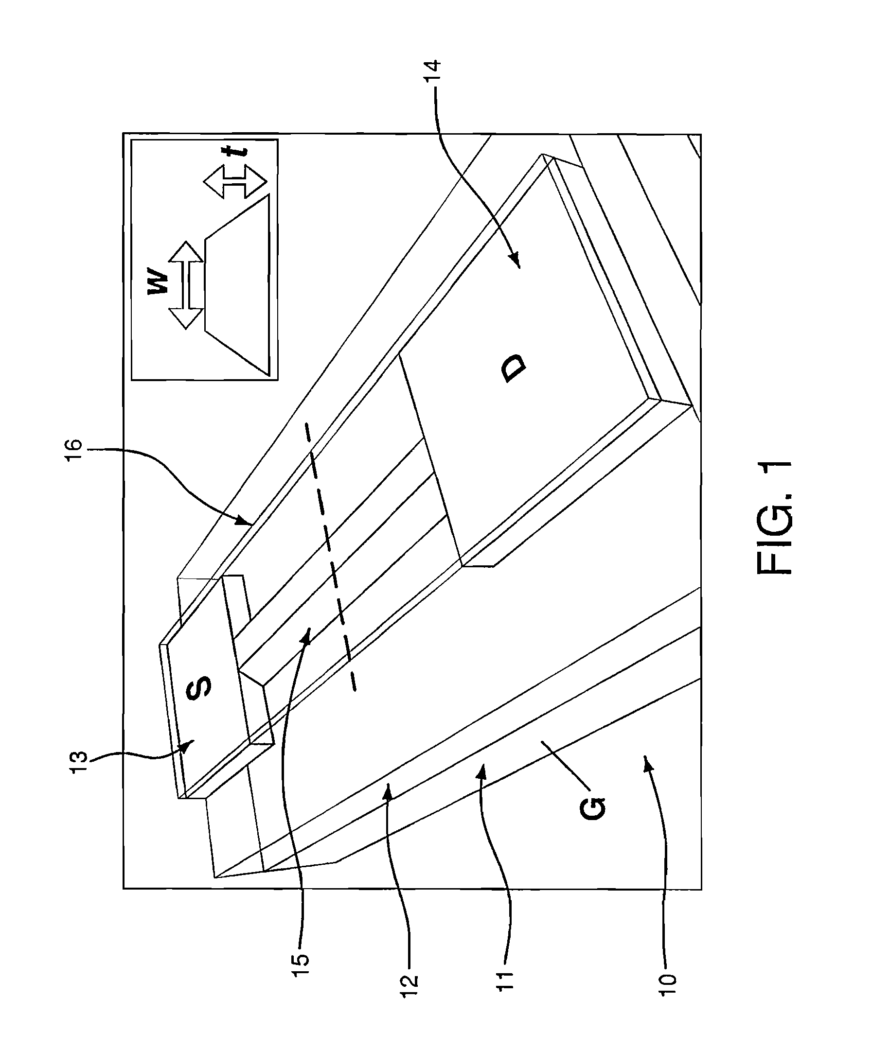
[0054]Certain preferred embodiments of the present invention provide devices, and methods for their production, especially suited to sense a variety of molecular species, biological species, or cellular responses. In this manner, the species and / or substances of-interest may be detected and / or monitored. These species or substances can be present in solid, liquid or gaseous state in the ambient or can be applied to the device. Sensors of the present invention, for example, are especially suited for detecting, measuring, or both, of proteins, DNA and intrinsic cellular changes or cellular changes due to extrinsic stimuli. Still further, sensors, as described and provided herein, may also be suitable for sensing cellular interactions due to paracrine, autocrine, or endocrine signaling, or combinations thereof. The detection device is implemented as an elongated nanostructure, for example, a nano-wire, and has an exposed surface that is substantially smooth and well defined. The nanost...
PUM
| Property | Measurement | Unit |
|---|---|---|
| width | aaaaa | aaaaa |
| thickness | aaaaa | aaaaa |
| width | aaaaa | aaaaa |
Abstract
Description
Claims
Application Information