Self-aligned process for fabricating voltage-gated MRAM
a voltage-gated memory and self-aligning technology, applied in digital storage, instruments, semiconductor devices, etc., can solve the problems of unrecordable elements, information readout errors increase, value change, etc., and achieve the effect of reducing the switching energy barrier of the recording layer and being easily switched or reversed
- Summary
- Abstract
- Description
- Claims
- Application Information
AI Technical Summary
Benefits of technology
Problems solved by technology
Method used
Image
Examples
first embodiment
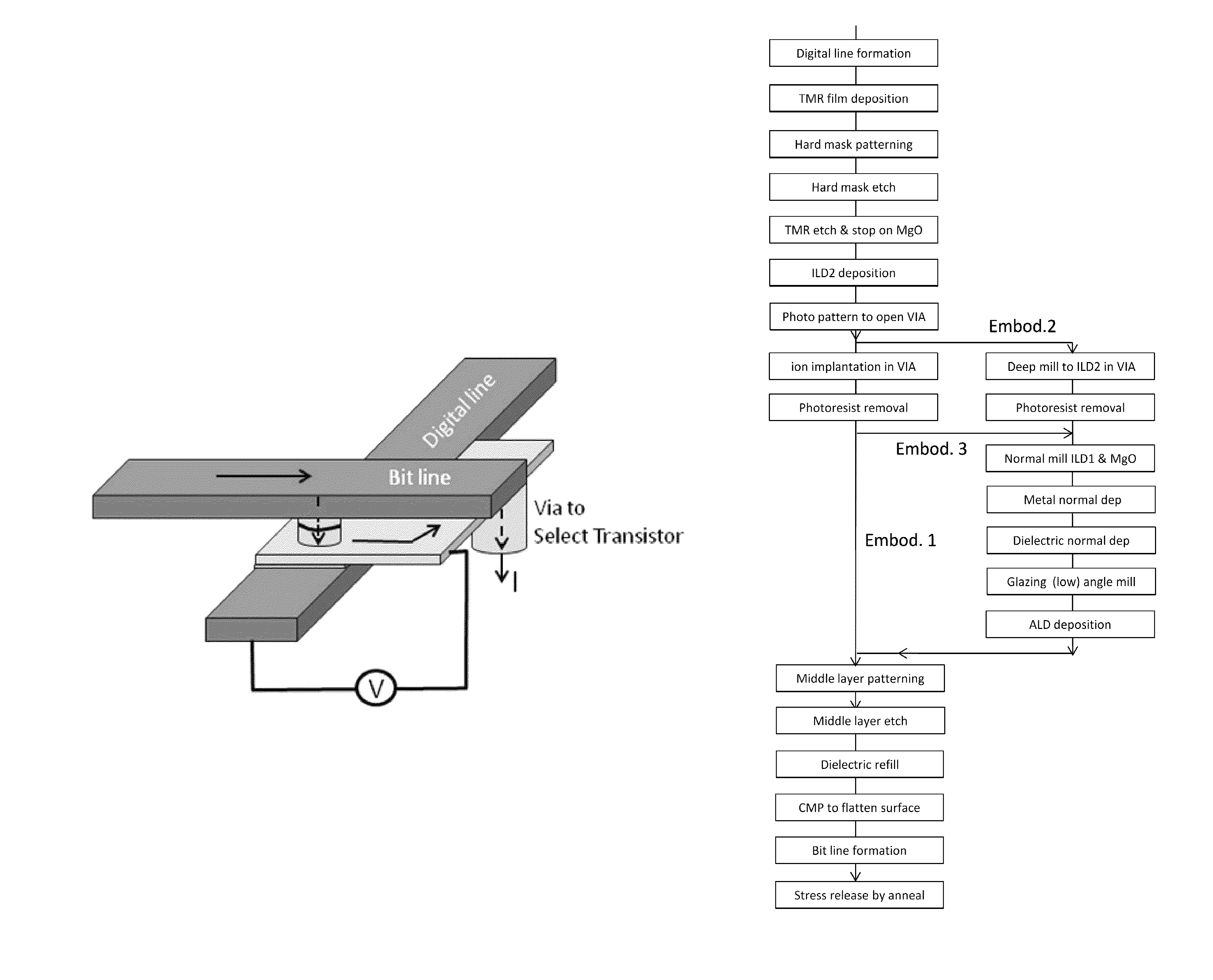
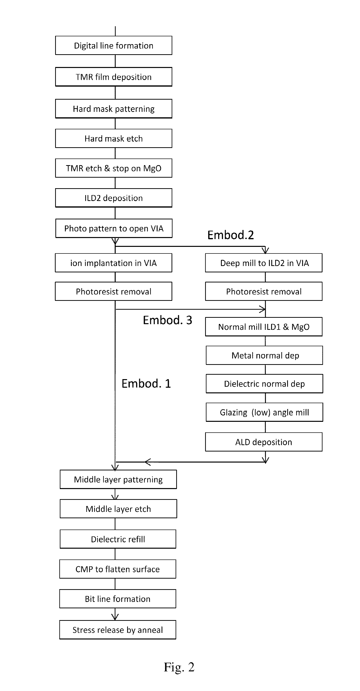
[0054]In a first method, a photolithography patterning is used to open the VIA, Then using the patterned photoresist as a mask, a metal (typically, Li, Cu, Au, Pt) ion implantation is used to add highly conductive metallic atoms deep into the buried ILD1 layer 310 to convert it into an electrically conducting layer (FIG. 7).
[0055]After ion implantation, the photoresist is removed, as shown in FIG. 8. Another photolithography patterning and etching process is used to electrically separate adjacent magnetoresistive cells and leave a conducting path between the middle memory cell and the VIA (FIG. 9, A—cross section, B—top view), followed by a refilling of a dielectric (typically SiO2) layer 395 and a CMP process to flatten the device surface, as shown in FIG. 10.
second embodiment
[0056]Following the photolithography patterning of VIA as described in the first embodiment, a deep etch by using low angle ion mill is used to remove all the materials (ILD1, MgO, middle memory and ILD2) from the VIA, as shown in FIG. 11. After removing the remaining photoresist, a low-angle normal (perpendicular) ion milling is used to remove the ILD1 and MgO across the wafer flat surface while keeping the vertical surfaces near MTJ junction of the memory pillar still partially covered by the remaining ILD2 layer, as shown in FIG. 12. Then a metal layer (typically Ru, Cu, Cu and Al alloy) is deposited over the entire surface including the etched VIA area, as shown in FIG. 13, which later on acts an electrical conducting path between the middle memory layer and the VIA to the underneath CMOS.
third embodiment
[0057]Continuing from embodiment one (see FIG. 8) a normal (perpendicular) ion milling is used to remove the ILD2 and MgO barrier layers from the flat surface while keeping the vertical surface where the memory pillar located still covered by a portion of ILD2, as shown in FIG. 14. Then a metal layer 385 (typically Ru, Cu, Cu and Al alloy) is normally deposited over the entire device surface, as shown in FIG. 15 for the purpose of electrical conducting enhancement between the middle memory layer and VIA to the underneath CMOS.
[0058]For the second and third embodiments, after a metal layer 385 deposition, a thin dielectric layer 388, such as SiO2, Si3N4 or Al2O3, is deposited to cover the top metal surface (as shown in FIG. 15), and a glazing (large) angle mill is used to remove the metal layer from the vertical surfaces near the MTJ junction on the memory pillar to prevent shorting, as shown in FIG. 16.
[0059]Similar to embodiment one, a photolithography patterning and etch is used t...
PUM
 Abstract
Description
Claims
Application Information


