
Method to make three-terminal MRAM

a three-terminal, memory technology, applied in the direction of magnetic field-controlled resistors, galvano-magnetic material selection, semiconductor devices, etc., can solve the problems of information readout errors increasing, value changes, and element unrecordable, so as to reduce the switching energy barrier of the recording layer, the effect of reducing the switching energy barrier

Inactive Publication Date: 2016-03-03
T3MEMORY
View PDF0 Cites 3 Cited by
  • Summary
  • Abstract
  • Description
  • Claims
  • Application Information

AI Technical Summary

Benefits of technology

The patent describes a memory cell that can read and write information using a special technology called magnetoresistive memory. The cell includes a circuit that applies a current to the memory elements to change their state. The current creates a magnetic field that can be controlled to switch the memory elements. The technology allows for faster and more energy-efficient data storage and retrieval.

Problems solved by technology

More, even when the tunnel barrier does not immediately break down, if recording operations are repeated, the element may still become nonfunctional such that the resistance value changes (decreases) and information readout errors increase, making the element un-recordable.
Furthermore, recording is not performed unless a sufficient voltage or sufficient spin current is applied.
Accordingly, problems with insufficient recording arise before possible tunnel barrier breaks down.
However, patterning of small MTJ element leads to increasing variability in MTJ resistance and sustaining relatively high switching current or recording voltage variation in a STT-MRAM.
Any fluctuation in the electrical characteristics of individual MTJs at advanced technology nodes could cause what was intended as a read-current, to have the effect of a write-current, thus unintentionally reversing the direction of magnetization of the recording layer in MTJ.
Above issues or problems are all associated with the traditional two-terminal MRAM configuration.

Method used


Image

  • Method to make three-terminal MRAM
  • Method to make three-terminal MRAM
  • Method to make three-terminal MRAM

Examples


Embodiment Construction

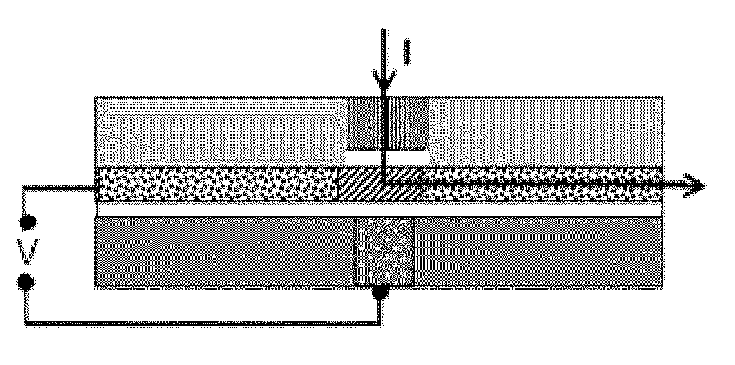
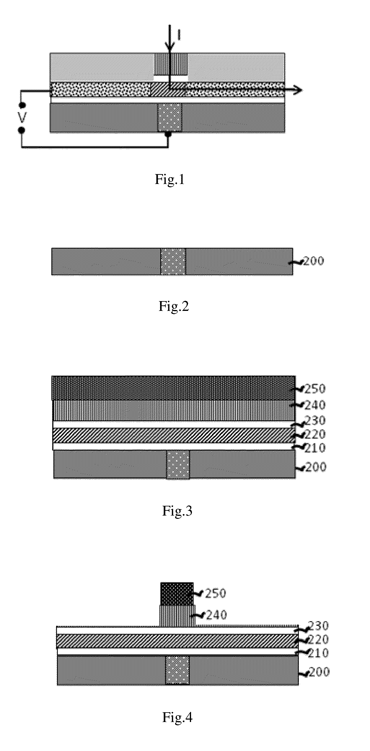
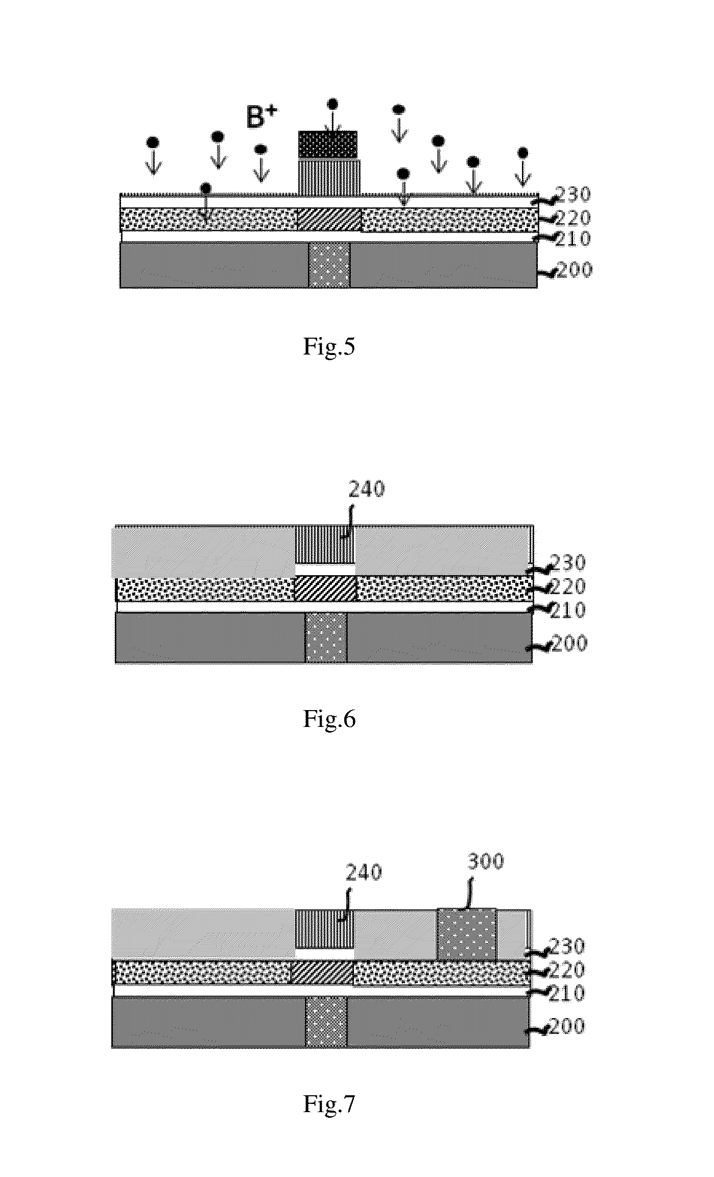
[0023]The three-terminal spin transfer torque transistor magnetic random access memory (ST3-MRAM) contains a digital line at the bottom, a bit line on the top, and a magnetic memory cell in the middle (FIG. 1). The middle memory cell has a bottom insulating layer (ILD), a magnetic memory layer, a dielectric MgO tunneling layer and a top magnetic reference layer. The top reference layer has perpendicular magnetization to the plane, and the polarization of the middle memory layer can be either perpendicular to the plane or in the plane depending on the voltage applied to the middle memory layer across the bottom ILD layer. Both read and write current flow through the top reference layer and middle memory layer. The digital line has a small contact area with the insulating layer below the memory cell which helps to reduce writing current when a voltage pulse is applied.

[0024]A device substrate (FIG. 2) contains a VIA (200) in the middle which is connected to the bottom CMOS control cir...


PUM


Abstract

This invention is about a method to make three-terminal spin transfer torque transistor magnetic random access memory (ST3-MRAM) cell using plasma based ion implantation. The core memory stack of such ST3-MRAM cell contains a bottom digit line (or VIA), a thick dielectric insulating layer, a memory layer, another thin dielectric layer, and a magnetic reference layer on the top. After the formation of the top magnetic reference pillar by photolithography patterning and etching, the outside region of the magnetic memory layer is converted to a non-magnetic conducting lead by heavy doping of boron ions generated by plasma from boron hydrogen (BxH3x) containing gas.

Description

RELATED APPLICATIONS[0001]This application claims the priority benefit of U.S. Provisional Application No. 61 / 874,029 filed on Sep. 5, 2013, which is incorporated herein by reference.BACKGROUND OF THE INVENTION[0002]1. Field of the Invention[0003]This invention relates generally to a three terminal magnetic-random-access memory (MRAM) cell, more particularly to the method of fabricating three terminal MRAM memory elements.[0004]2. Description of the Related Art[0005]In recent years, magnetic random access memories (hereinafter referred to as MRAMs) using the magnetoresistive effect of ferromagnetic tunnel junctions (also called MTJs) have been drawing increasing attention as the next-generation solid-state nonvolatile memories that can also cope with high-speed reading and writing. A ferromagnetic tunnel junction has a three-layer stack structure formed by stacking a recording layer having a changeable magnetization direction, an insulating tunnel barrier layer, and a fixed layer th...

Claims


Application Information

Patent Timeline
IPC IPC(8): H01L43/08H01L43/02H01L43/10H01L43/12
CPCH01L43/08H01L43/12H01L43/10H01L43/02H10N50/01H10N50/10
Inventor GUO, YIMIN
Owner T3MEMORY
Learn More