Semiconductor device and manufacturing method thereof

a technology of semiconductor devices and semiconductor balls, applied in semiconductor devices, semiconductor/solid-state device details, electrical apparatus, etc., can solve the problems of reducing the reliability of solder bonding on the board, cracking at the edge of the surface where solder balls are placed, and oxidizing the surface easily, etc., to achieve excellent malleability and ductility.

Active Publication Date: 2015-09-01
AMKOR TECH SINGAPORE HLDG PTE LTD
View PDF32 Cites 5 Cited by
  • Summary
  • Abstract
  • Description
  • Claims
  • Application Information

AI Technical Summary

Benefits of technology

[0012]Since the nickel plated layer has excellent malleability and ductility, the nickel plated layer prevents cracking of the first copper plated layer from stress applied to the solder ball. Further, the nickel plated layer provides a barrier layer for preventing the first copper plated layer from reacting with the solder ball.

Problems solved by technology

However, since copper (Cu) easily responds to oxygen in the atmosphere as is widely well known, its surface is easily oxidized during a high temperature hardening process, etc.
However, conventional WLCSPs comprise solder balls formed on just right surfaces of wafers so that mechanical stress transferred from outside is delivered to solder balls, which drops a board level reliability including solder bonding.
In this regard, since redistribution layers have a monotonous structure using plated copper (Cu), they cannot absorb external shocks, which causes a crack at an edge of surfaces where solder balls and redistribution layers contact.

Method used


Image

  • Semiconductor device and manufacturing method thereof
  • Semiconductor device and manufacturing method thereof
  • Semiconductor device and manufacturing method thereof

Examples


Embodiment Construction

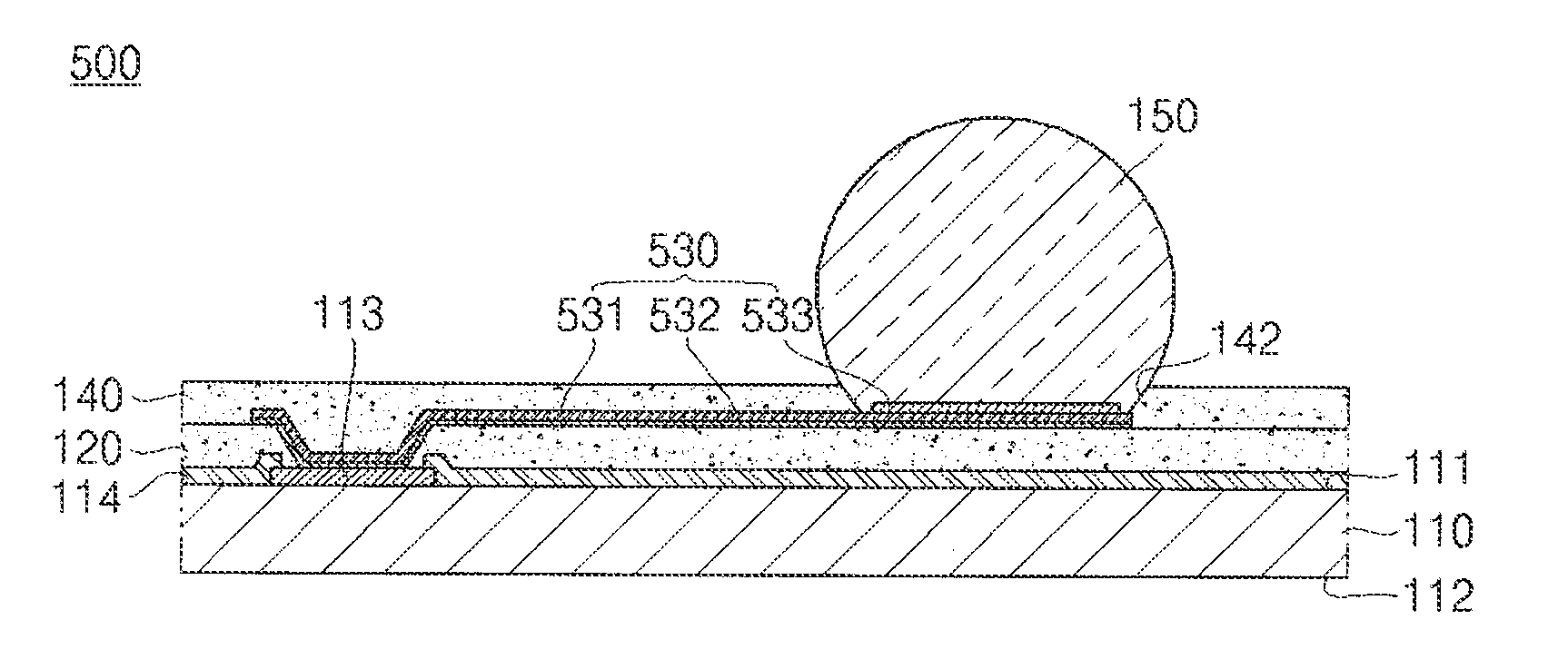
[0033]Referring to FIG. 1, a cross-sectional view of a semiconductor device 100 according to an embodiment of the present invention is shown.

[0034]As shown in FIG. 1, the semiconductor device 100 of the present embodiment of the present invention comprises a semiconductor die 110, a first dielectric layer 120, a redistribution layer 130, a second insulating layer 140, and a solder ball 150.

[0035]The semiconductor die 110 has a first surface 111 that is roughly flat and a second surface 112 that is also roughly flat on the opposite side of the first surface 111. At least one bond pad 113 can be formed on the first surface 111 of the semiconductor die 110. Furthermore, a passivation layer 114 can be formed on the first surface 111 that is a circumferential surface of the bond pads 113.

[0036]The passivation layer 114 can be formed of Polylmide (PI), Benzo Cyclo Butene (BCB), Poly Benz Oxazole (PBO), BismaleimideTriazine (BT), phenolic resin, epoxy, Silicone (Si), silicon oxide film (Si...


PUM

PropertyMeasurementUnit
thicknessaaaaaaaaaa
thicknessaaaaaaaaaa
thicknessaaaaaaaaaa

Abstract

A semiconductor device and method of manufacturing the same are provided. The semiconductor device comprises a semiconductor die including a bond pad, a redistribution layer, and a solder ball. The redistribution layer is formed by sequentially plating copper and nickel, sequentially plating nickel and copper, or sequentially plating copper, nickel, and copper. The redistribution layer includes a nickel layer in order to prevent a crack from occurring in a copper layer. Further, a projection is formed in an area of the redistribution layer or a dielectric layer to which the solder ball is welded and corresponds, so that an area of the redistribution layer to which the solder ball is welded increases, thereby increasing bonding power between the solder ball and the redistribution layer.

Description

RELATED APPLICATIONS[0001]This application is a divisional of Jin et al., U.S. patent application Ser. No. 12 / 116,695, filed on May 7, 2008, entitled “SEMICONDUCTOR DEVICE HAVING REDISTRIBUTION LAYER”, now U.S. Pat. No. 8,058,726, issued on Nov. 15, 2011, which is herein incorporated by reference in its entirety.BACKGROUND OF THE INVENTION[0002]1. Field of the Invention[0003]The present invention relates to a semiconductor device and a method of manufacturing the same.[0004]2. Description of the Related Art[0005]Chip size packages (CSPs) are generally completed directly after each of semiconductor-processed wafers is singulated into a semiconductor chip. However, wafer level packages (WLPs) are completed after circuit is redistributed or is flip-chip bumped in a wafer state and then is singulated. Therefore, wafer level chip size packages (WLCSPs) are processed in a wafer level and have the same size as the semiconductor chip.[0006]WLCSPs are processed in a wafer level and have the ...

Claims


Application Information

Patent Timeline
Patent Type & Authority Patents(United States)
IPC IPC(8): H01L23/48H01L23/52H01L23/00
CPCH01L24/05H01L23/3192H01L24/03H01L24/11H01L24/13H01L2224/0239H01L2224/03828H01L2224/0401H01L2224/05548H01L2224/05571H01L2224/05647H01L2224/11849H01L2224/13022H01L2224/13111H01L2924/01029H01L2924/0103H01L2924/01082H01L2924/014H01L2924/01005H01L2924/01006H01L2924/01033H01L2924/01047H01L2924/0105H01L2224/05558H01L2924/0002H01L2224/05552H01L2924/181H01L2224/05556H01L2224/13006H01L2224/05557H01L2224/0236H01L2224/02351H01L2224/02125H01L2924/00H01L2924/00012
Inventor JIN, JUNG GIPAEK, JONG SIKPARK, SUNG SUKIM, SEOK BONGHWANG, TAE KYUNGCHA, SE WOONG
Owner AMKOR TECH SINGAPORE HLDG PTE LTD
Why Eureka
Try Eureka