Sensing apparatus

a technology of sensing apparatus and etching process, which is applied in the direction of transistors, solid-state devices, radio-controlled devices, etc., can solve the problems of high manufacturing cost, large thickness of conventional image sensing array, and significant time spent on pin layer depositing, so as to reduce the number of times of photolithography and etching process for forming the sensing apparatus.

Active Publication Date: 2015-11-17
AU OPTRONICS CORP
View PDF4 Cites 5 Cited by
  • Summary
  • Abstract
  • Description
  • Claims
  • Application Information

AI Technical Summary

Benefits of technology

[0007]The invention is directed to a sensing apparatus which is suitable for a large area fabrication, and the number of times of performing photolithography and etching processes (PEPs) for forming the sensing apparatus can be reduced.
[0009]Accordingly, in the sensing apparatus described herein, the sensing device senses light through a junction constituted by the amorphous silicon layer and the graphene layer, and thereby the sensing apparatus can be suitable for the large area production. In addition, the sensing apparatus described herein may be manufactured by performing the reduced number of PEPs, such that the complexity of the overall manufacturing process and the manufacturing costs can be both reduced.

Problems solved by technology

As a result, the conventional image sensing array not only has the large thickness but also requires significant time spent on depositing the PIN layer and high manufacturing costs.
Besides, the conventional image sensing array can be completely formed by performing eleven photolithography and etching processes (PEPs) in most cases, which further complicates the manufacturing process.

Method used


Image

  • Sensing apparatus
  • Sensing apparatus
  • Sensing apparatus

Examples


Embodiment Construction

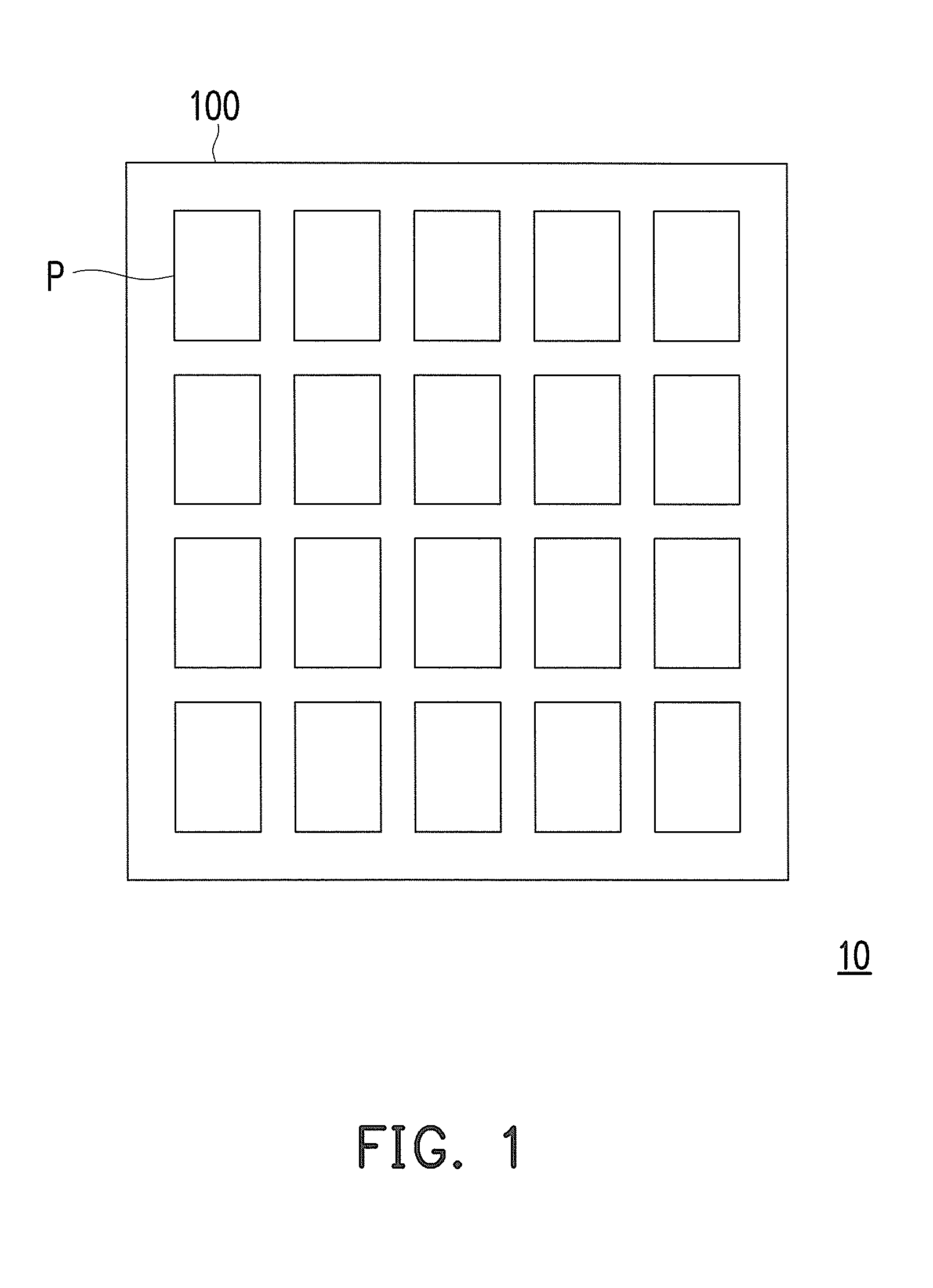
[0018]FIG. 1 is a schematic top view illustrating a sensing apparatus according to an embodiment of the invention.

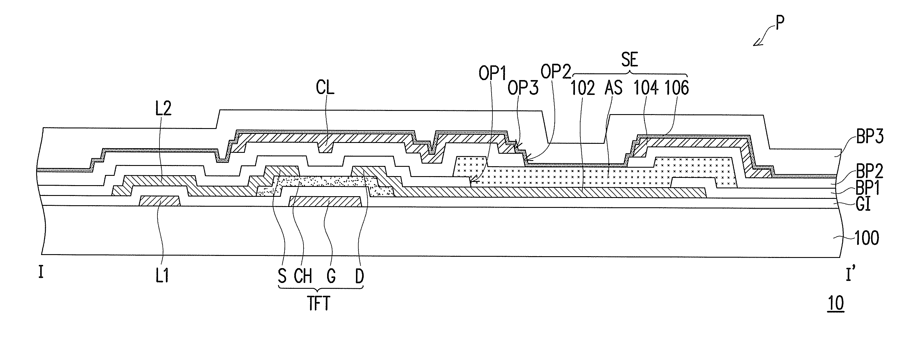
[0019]With reference to FIG. 1, the sensing apparatus 10 includes a substrate 100 and a plurality of sensing pixels P. The substrate 100 is made of glass, quartz, organic polymer, an opaque / reflective material (e.g., a conductive material, metal, wafer, ceramics, or any other appropriate material), or any other appropriate material. The sensing pixels P are located on the substrate 100.

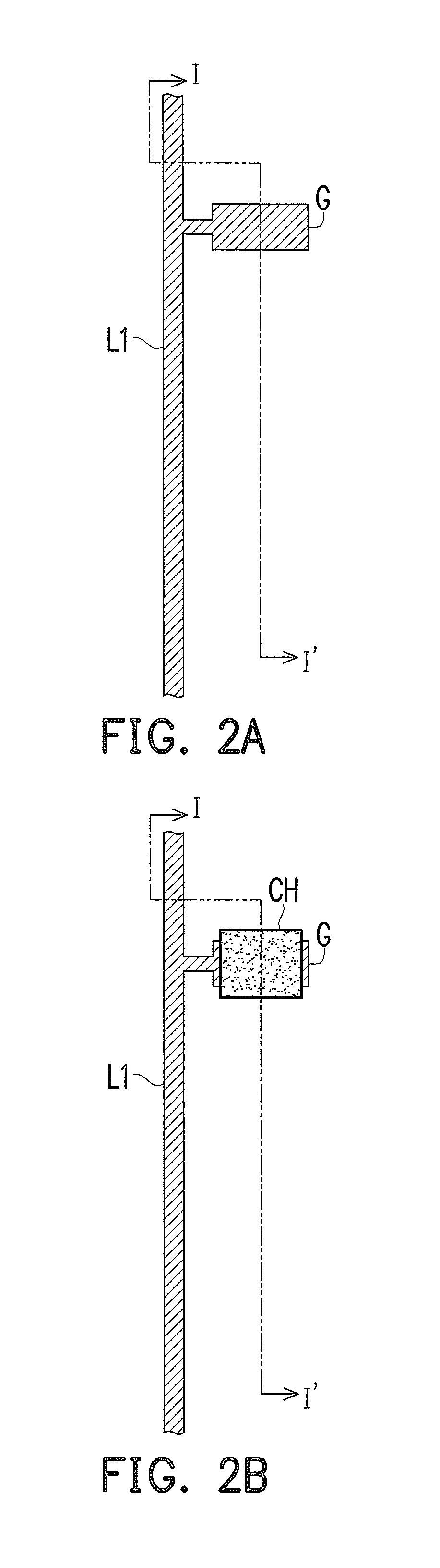
[0020]The manufacturing method of the sensing apparatus 10 will be elaborated hereinafter with reference to FIG. 2A to FIG. 2H and FIG. 3A to FIG. 3H. Note that the sensing apparatus 10 includes a plurality of sensing pixels P, and the sensing pixels P are adjacent to each other and are arranged in columns and rows to form an array. However, for illustrative purposes, FIG. 2A to FIG. 2H and FIG. 3A to FIG. 3H merely show one of the sensing pixels P in the sensing apparatus 10.

[0021]FIG. 2A...


PUM


Abstract

A sensing apparatus that includes a plurality of sensing pixels is provided. The sensing pixels are arranged in an array, and each of the sensing pixels includes an active device and a sensing device. The sensing device is electrically connected to the active device, and the sensing device includes a first electrode layer, an amorphous silicon layer, a second electrode layer, and a graphene layer. The amorphous silicon layer is located on the first electrode layer. The second electrode layer is located on the amorphous silicon layer and has an opening. The graphene layer is in contact with the second electrode layer and the amorphous silicon layer.

Description

CROSS-REFERENCE TO RELATED APPLICATION[0001]This application claims the priority benefit of Taiwan application serial no. 103122336, filed on Jun. 27, 2014. The entirety of the above-mentioned patent application is hereby incorporated by reference herein and made a part of this specification.BACKGROUND[0002]1. Field of the Invention[0003]The invention relates to a sensing apparatus; more particularly, the invention relates to a sensing apparatus in which a sensing device includes an amorphous silicon layer and a graphene layer.[0004]2. Description of Related Art[0005]In the existing image sensing array, each sensing pixel usually includes one thin film transistor (TFT) and one PIN diode. The TFT serves as a switch device performing a reading function, and the PIN diode acts as a sensing device which converts optical energy into electronic signals.[0006]Generally, in order for the image sensing array to achieve remarkable quantum efficiency (QE), i.e., incident photon-to-electron con...

Claims


Application Information

Patent Timeline
Patent Type & Authority Patents(United States)
IPC IPC(8): H01L27/146H01L31/0224H01L31/105H01L31/0376H01L31/028H01L29/786
CPCH01L27/14643H01L27/14616H01L29/78669H01L31/028H01L31/03762H01L31/1055H01L31/022408H01L27/14636H01L27/14665H01L27/14603H01L27/14692H01L27/1214Y02E10/547
Inventor CHEN, TSUNG-HANLIN, CHIN-MAO
Owner AU OPTRONICS CORP
Why Eureka
Try Eureka