Memory cell and manufacturing method thereof

a memory cell and manufacturing method technology, applied in the field of memory cells, can solve the problems of reducing the performance of the memory, flash memory may suffer from affecting the reliability of the device, etc., and achieve the effect of reducing the generation of a second bit effect and program disturbance during operation

Active Publication Date: 2015-12-08
MACRONIX INT CO LTD
View PDF4 Cites 0 Cited by
  • Summary
  • Abstract
  • Description
  • Claims
  • Application Information

AI Technical Summary

Benefits of technology

[0008]The embodiments of the invention provide a memory cell capable of reducing the generation of a second bit effect and program disturbance during operation.
[0009]The embodiments of the invention also provide a manufacturing method of a memory cell. The manufacturing method can be integrated with a current manufacturing process, and the manufactured memory cell can reduce the issues of the second bit effect and program disturbance.
[0030]Based on the above, in the memory cell of the invention, the isolation structure is formed in the substrate before the doped regions of the first conductivity type, the doped region of the second conductivity type, and the stacked structures are formed. The top surface of the isolation structure is in direct contact with the bottom surface of each of the doped regions of the first conductivity type and the bottom surface of the doped region of the second conductivity type, and therefore the travelling path of an electron from a charge trapping layer in the stacked structures to a charge trapping layer of an adjacent memory cell can be effectively blocked. As a result, program disturbance in the memory can be effectively prevented.
[0031]Moreover, since two storage locations of each of the memory cells are isolated from each other and the region for storage (also referred to as a capture region) is very small, the second bit effect can be reduced.
[0032]Moreover, the manufacturing process of the memory cell of the embodiments of the invention does not require an excess number of additional process steps and can be integrated with a current manufacturing process to manufacture a memory cell capable of reducing the issues of the second bit effect or program disturbance.

Problems solved by technology

However, if the tunnel oxide layer under the polysilicon floating gate has a defect, a leakage current can be readily generated in the device and affect the reliability of the device.
However, a flash memory may suffer from a second bit effect.
In addition, the length of a channel is reduced as the memory is miniaturized, which makes the second bit effect more significant, thereby reducing the performance of the memory.
As a result, program disturbance may readily occur and affect the reliability of the memory device when a programming operation is performed on a neighboring memory.

Method used


Image

  • Memory cell and manufacturing method thereof
  • Memory cell and manufacturing method thereof
  • Memory cell and manufacturing method thereof

Examples


first embodiment

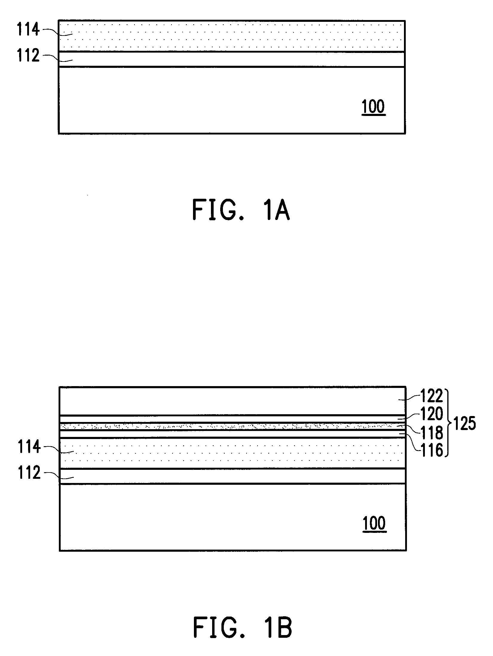
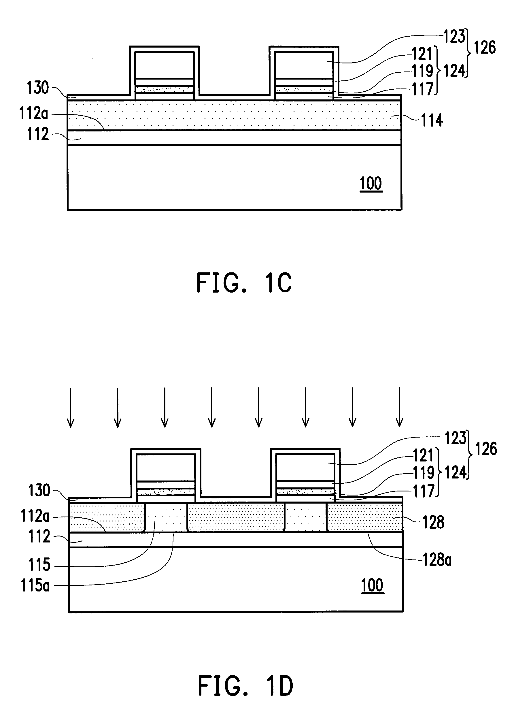
[0038]FIG. 1A to FIG. 1E are schematic cross-sectional diagrams of a manufacturing process of a non-volatile memory device illustrated according to the invention.

[0039]In the following, the first conductivity type is N-type and the second conductivity type is P-type for illustration. However, the invention is not limited thereto. Those having ordinary skill in the art should know that the first conductivity type can also be changed to P-type and the second conductivity type be changed to N-type. In particular, the N-type dopant is, for instance, phosphorous or arsenic, and the P-type dopant is, for instance, boron or boron difluoride (BF2).

[0040]First, referring to FIG. 1A, an isolation structure 112 is formed on a substrate 100. The substrate 100 can be formed by at least one semiconductor material selected from the group consisting of Si, Ge, SiGe, GaP, GaAs, SiC, SiGeC, InAs, and InP. The material of the isolation structure 112 is, for instance, any suitable material such as sili...

second embodiment

[0054]FIG. 2A to FIG. 2E are schematic cross-sectional diagrams of a manufacturing process of a non-volatile memory device illustrated according to the invention. The manufacturing process of the semiconductor device of FIG. 2A to FIG. 2E is similar to the manufacturing process of the non-volatile memory device of FIG. 1A to FIG. 1E, and therefore the same elements are represented by the same labels and are not repeated herein.

[0055]First, referring to FIG. 2A, a plurality of isolation structures 212 are formed in a substrate 100. In the figure, only two isolation structures 212 are illustrated. A depth H2 of each of the isolation structures 212 is, for instance, 500 angstroms to 3000 angstroms. The material of the isolation structures 212 is, for instance, any suitable material such as silicon oxide, silicon oxynitride, silicon carbide, or silicon carbon nitride. The forming method of the isolation structures 212 is, for instance, a shallow trench isolation method or a deep trench ...

third embodiment

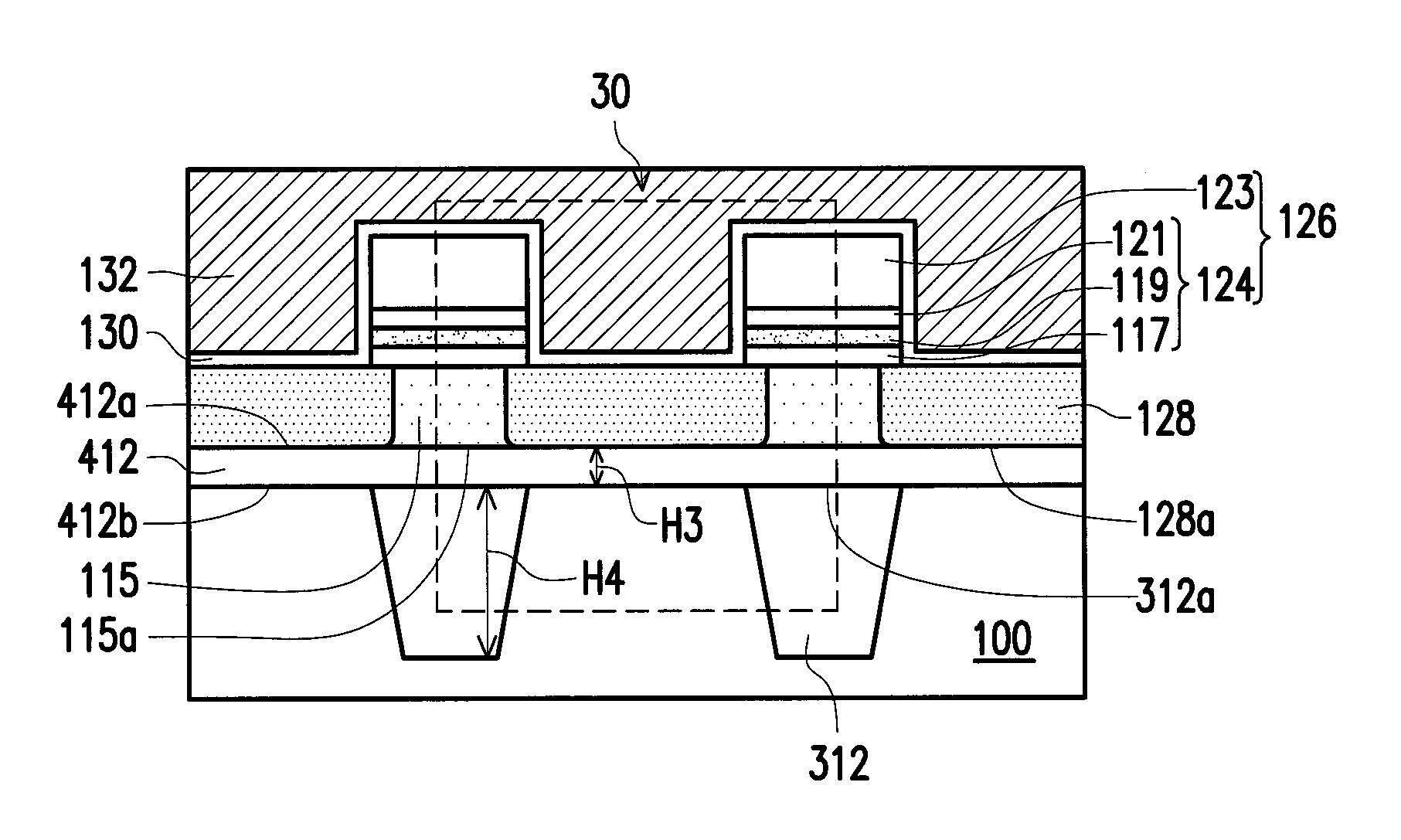
[0061]FIG. 3A to FIG. 3F are schematic cross-sectional diagrams of a manufacturing process of a non-volatile memory device illustrated according to the invention. The manufacturing process of the semiconductor device of FIG. 3A to FIG. 3F is similar to the manufacturing process of the non-volatile memory device of FIG. 1A to FIG. 1E, and therefore the same elements are represented by the same labels and are not repeated herein.

[0062]First, referring to FIG. 3A, isolation structures 312 are formed in a substrate 100. The material of the isolation structures 312 is, for instance, any suitable material such as silicon oxide, silicon oxynitride, silicon carbide, or silicon carbon nitride. A depth H4 of each of the isolation structures 312 is, for instance, 500 angstroms to 3000 angstroms. The forming method of the isolation structures 312 is, for instance, a shallow trench isolation method or a deep trench isolation method.

[0063]Then, referring to FIG. 3B, an isolation structure 412 is ...


PUM


Abstract

Provided is a memory cell including a substrate, two doped regions of a first conductivity type, one doped region of a second conductivity type, two stacked structures, and a first isolation structure. The doped regions of the first conductivity type are respectively disposed in the substrate. The doped region of the second conductivity type is disposed in the substrate between the two doped regions of the first conductivity type. The stacked structures are disposed on the substrate and respectively cover the corresponding doped regions of the first conductivity type and a portion of the doped region of the second conductivity type. Each of the stacked structures includes one charge storage layer. The first isolation structure completely covers and is in contact with the bottom surface of each of the doped regions of the first conductivity type and the bottom surface of the doped region of the second conductivity type.

Description

BACKGROUND OF THE INVENTION[0001]1. Field of the Invention[0002]The invention is related to a memory cell and a manufacturing method thereof.[0003]2. Description of Related Art[0004]A memory is a semiconductor device designed for the purpose of storing information or data. As the functionalities of computer microprocessors become more and more powerful, programs and operations executed by software are increasing correspondingly. As a consequence, the demand for a memory is ever increasing. Among various memory devices, the non-volatile memory has the advantage of retaining stored data after being disconnected. Therefore, many electronic products require the non-volatile memory to maintain normal operation when the electronic products are turned on.[0005]A typical non-volatile memory has a floating gate and a control gate fabricated by using doped polysilicon. As the memory is programmed, electrons injected into the floating gate can be uniformly distributed in the entire polysilicon...

Claims


Application Information

Patent Timeline
Patent Type & Authority Patents(United States)
IPC IPC(8): H01L27/115H01L29/792H01L29/66
CPCH01L27/11568H01L29/66833H01L29/792H01L21/762H01L29/7923H01L21/76224H10B43/30
Inventor CHENG, CHIH-CHIEHYAN, SHIH-GUEITSAI, WEN-JER
Owner MACRONIX INT CO LTD
Why Eureka
Try Eureka