Method of photoresist strip

Active Publication Date: 2016-01-05
CHIPBOND TECH
View PDF17 Cites 0 Cited by
  • Summary
  • Abstract
  • Description
  • Claims
  • Application Information

AI Technical Summary

Benefits of technology

The present invention describes a method for stripping photoresist from a semiconductor substrate using a flow scouring process. The method reduces the time the substrate is immersed in the chemical solution, resulting in lower costs and higher yield rates for semiconductor device fabrication. The method also prevents damage to the substrate or other components, improving the overall process quality.

Problems solved by technology

For the issue mentioned above, in the process of conventional photoresist strip, the time for immersing the substrate into the photoresist stripping solution is likely too long therefore causing dispersion of the bumps or damage of a protection layer of the substrate.
Oppositely, once the time for immersing the substrate into the photoresist stripping solution is too short, the remaining of the photoresist layer is likely occurred therefore affecting the yield rate in the conventional bump process.
The thicker photoresist layer need longer time for immersed into the photoresist stripping solution and more photoresist stripping solution for strip which increase the loading capacity of the environmental and producing cost.

Method used


Image

  • Method of photoresist strip
  • Method of photoresist strip
  • Method of photoresist strip

Examples


Embodiment Construction

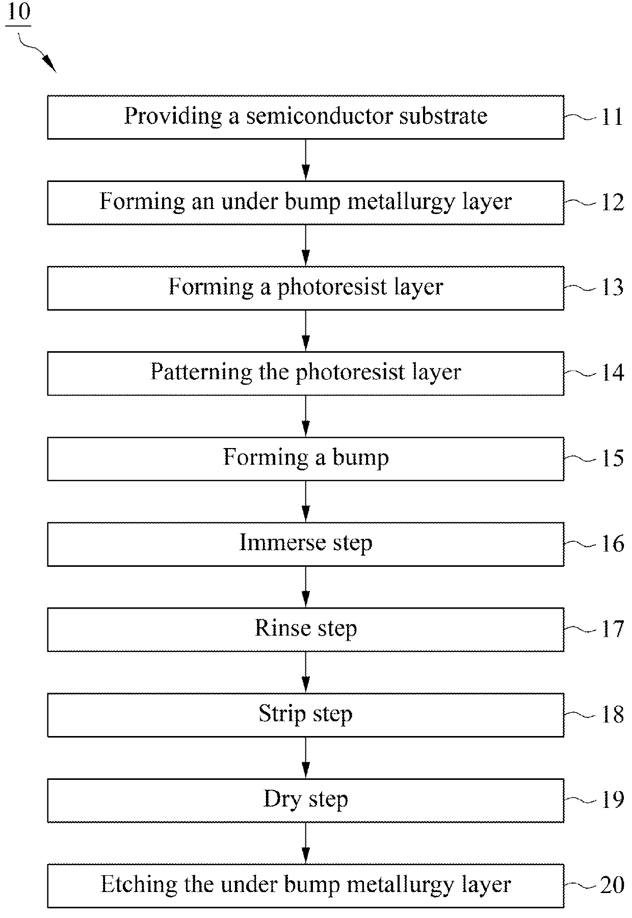
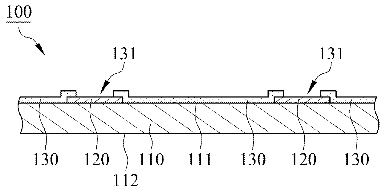
[0010]A method of photoresist strip 10 in accordance with a first embodiment of the present invention is illustrated in a flow chart of FIG. 1. With reference to FIGS. 1 and 2, the step 11 of providing a semiconductor substrate provides a semiconductor substrate 100, wherein the semiconductor substrate 100 comprises a base 110, a bonding pad 120 and a protective layer 130, the bonding pad 120 located at a surface 111 of the base 110 is selected from copper, aluminum, copper alloy or other conductive material, the protective layer 130 covers the base 110 and the bonding pad 120 and comprises an opening 131 to reveal the bonding pad 120.

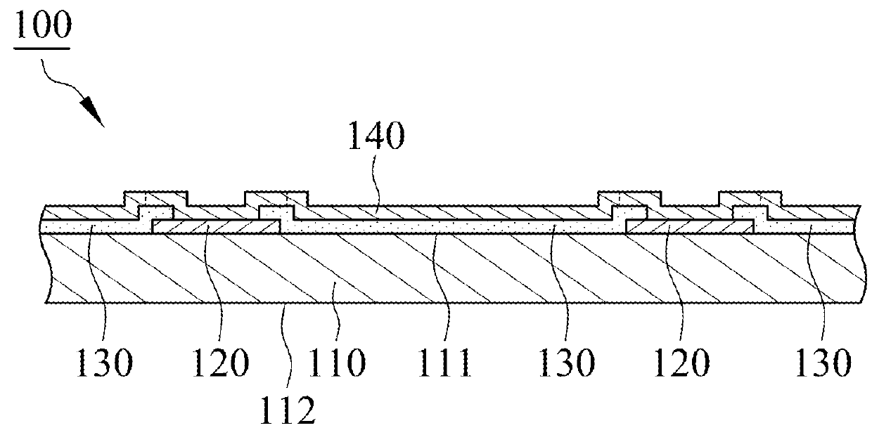
[0011]With reference to FIGS. 1 and 3, in the step 12 of forming an under bump metallurgy layer, an under bump metallurgy layer 140 is plated onto the protective layer 130 by evaporation, sputtering, electroplating or electroless plating. The under bump metallurgy layer 140 covers the protective layer 130 and connects to the bonding pad 120, wherein th...


PUM


Abstract

A method of photoresist strip includes providing a semiconductor substrate and performing an immerse step and a strip step, wherein the semiconductor substrate comprises a base, a bonding pad, a protective layer, an under bump metallurgy layer, a patterned photoresist layer and a bump. The patterned photoresist layer covers the under bump metallurgy layer and a lateral surface of the bump, wherein a first connection interface is formed between the patterned photoresist layer and the lateral surface of the bump, and a second connection interface is formed between the patterned photoresist layer and the under bump metallurgy layer. In the immerse step, the patterned photoresist layer contacts with a chemical solution which degrades the bond strength of the first connection interface. Therefore, in the strip step, the semiconductor substrate is scoured by a flow with appropriate force of impact, which strips the patterned photoresist layer from the base.

Description

FIELD OF THE INVENTION[0001]The present invention is generally relating to a method of photoresist strip, particularly to the method of photoresist strip for stripping photoresist by a flow.BACKGROUND OF THE INVENTION[0002]Conventional bump process includes forming a photoresist layer on a substrate; performing exposure / develop process to pattern the photoresist layer; plating plural bumps on the patterned photoresist layer; eventually removing the patterned photoresist layer therefore completing the bump process. In the process of removing the photoresist layer, the substrate which covered by the photoresist layer is immersed into a photoresist stripping solution to make the photoresist layer generate imbibition and decomposition therefore stripping from the substrate. However, according to differed product demands, the types of photoresist materials and photoresist stripping solutions used in process are totally different. For the issue mentioned above, in the process of conventio...

Claims


Application Information

Patent Timeline
IPC IPC(8): H01L21/44H01L21/311
CPCH01L21/311H01L21/31133H01L24/03H01L24/05H01L24/11H01L24/13H01L2224/02311H01L2224/02313H01L2224/02331H01L2224/0345H01L2224/03462H01L2224/03464H01L2224/0347H01L2224/03912H01L2224/03914H01L2224/05008H01L2224/05022H01L2224/05124H01L2224/05147H01L2224/05548H01L2224/05569H01L2224/05572H01L2224/0558H01L2224/1145H01L2224/11462H01L2224/11464H01L2224/1147H01L2224/1181H01L2224/13024H01L2224/13082H01L2224/13083H01L2224/13111H01L2224/13144H01L2224/13147H01L2224/13155H01L2924/00014H01L2924/00012H01L2924/01047H01L2924/014H01L2224/05599H01L21/0273
Inventor SHIH, CHENG-HUNGYANG, KUO-HUAHOU, HSIANG-PIN
Owner CHIPBOND TECH
Why Eureka
Try Eureka