
Trace stacking structure and method

a stacking structure and stacking technology, applied in the field of electronic components, can solve the problems of increasing the overall cost of the substrate, reducing the electrical performance of the traces, and forming the traces of high-grade electrically conductive materials is relatively expensive, and achieves a large current carrying cross-sectional area, small width, and small pitch

Active Publication Date: 2016-01-05
AMKOR TECH SINGAPORE HLDG PTE LTD
View PDF7 Cites 9 Cited by
  • Summary
  • Abstract
  • Description
  • Claims
  • Application Information

AI Technical Summary

Benefits of technology

The patent describes a way to make multiple small traces in a substrate that have a larger cross-sectional area for carrying electric current. This allows for high performance while keeping the traces narrow. This method also reduces the cost of manufacturing the substrate because it avoids using expensive materials.

Problems solved by technology

As the width of the traces is reduced, the cross-sectional area (the conductor volume) of the traces is reduced thus reducing the electrical performance of the traces.
However, forming the traces of the high-grade electrically conductive material is relatively expensive thus increasing the overall cost of substrate.

Method used


Image

  • Trace stacking structure and method
  • Trace stacking structure and method
  • Trace stacking structure and method

Examples


Embodiment Construction

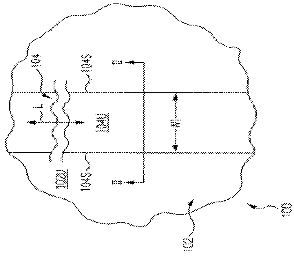
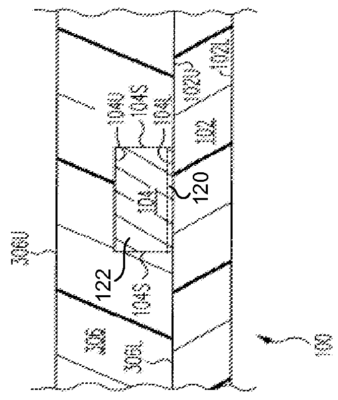
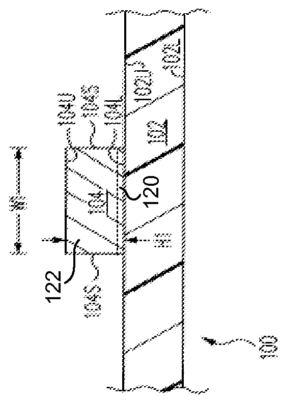
[0034]As an overview, referring to FIG. 5, a substrate 100 includes a stacked trace 524 formed from a trace 104 and a first buildup trace 516 stacked on trace 104. First buildup trace 516 contacts and is electrically connected to trace 104 along the entire length of trace 104.

[0035]Stacked trace 524 has width W1 equal to width W1 of trace 104. Further, stacked trace 524 has a height H3 equal to height H1 of trace 104 plus height H2 of first buildup trace 516. Accordingly, the current carrying cross-sectional area of stacked trace 524 is greater than the current carrying cross-sectional area of trace 104.

[0036]Accordingly, a plurality of stacked traces 524 can be formed with a small width W1 and thus small pitch yet with a large current carrying cross-sectional area. In this manner, stacked traces 524 have high electrical performance while at the same time have a minimum width W1. Further, in one embodiment, stacked traces 524 are formed without use of an expensive high-grade electri...


PUM


Abstract

A substrate includes a stacked trace formed from a trace and a first buildup trace stacked on the trace. The first buildup trace contacts and is electrically connected to the trace along the entire length of the trace. The current carrying cross-sectional area of the stacked trace is greater than the current carrying cross-sectional area of the trace. Accordingly, a plurality of the stacked traces can be formed with a small width and thus small pitch yet with a large current carrying cross-sectional area.

Description

BACKGROUND OF THE INVENTION[0001]1. Field of the Invention[0002]The present application relates to the field of electronics, and more particularly, to methods of forming electronic component packages and related structures.[0003]2. Description of the Related Art[0004]A substrate includes an electrically conductive circuit having various electrically conductive features. These electrically conductive features include, for example, traces, vias, terminals, and bond fingers.[0005]The traces of the circuit are long electrically conductive connectors that electrically connected the other features of the circuit. To form a high density circuit, the width and thus pitch of the traces is minimized. As the width of the traces is reduced, the cross-sectional area (the conductor volume) of the traces is reduced thus reducing the electrical performance of the traces. The cross-sectional area of a trace is sometimes called the current carrying cross-sectional area as it is the cross-sectional ar...

Claims


Application Information

Patent Timeline
Patent Type & Authority Patents(United States)
IPC IPC(8): H01L23/48
CPCH01L23/48H01L23/49822H01L23/49827H01L23/5389H01L23/552H01L24/16H01L24/19H01L24/20H01L24/73H01L2224/0401H01L2224/04105H01L2224/05571H01L2224/16237H01L2224/73267H01L2924/14H01L2924/15174H01L2924/15311H01L2924/15313H05K1/0265H05K2201/0379H01L2924/00012H01L21/4857H01L23/49838H01L23/66H01P3/02H05K3/10
Inventor HINER, DAVID JONHUEMOELLER, RONALD PATRICKMCCALEB, III, HARRY DONALDDEVITA, JR., MICHAEL HARRY
Owner AMKOR TECH SINGAPORE HLDG PTE LTD
Learn More