Mutual capacitance large panel phase shift mitigation

a phase shift mitigation and capacitance technology, applied in the field of touch screens, can solve the problems of amplification of errors, less perfect estimation of capacitance values, and measurable change in capacitance, and achieve the effect of reducing the integrated circuit area and power consumption of touch controllers, and large phase shifts

Active Publication Date: 2016-01-12
QUALCOMM INC
View PDF13 Cites 17 Cited by
  • Summary
  • Abstract
  • Description
  • Claims
  • Application Information

AI Technical Summary

Benefits of technology

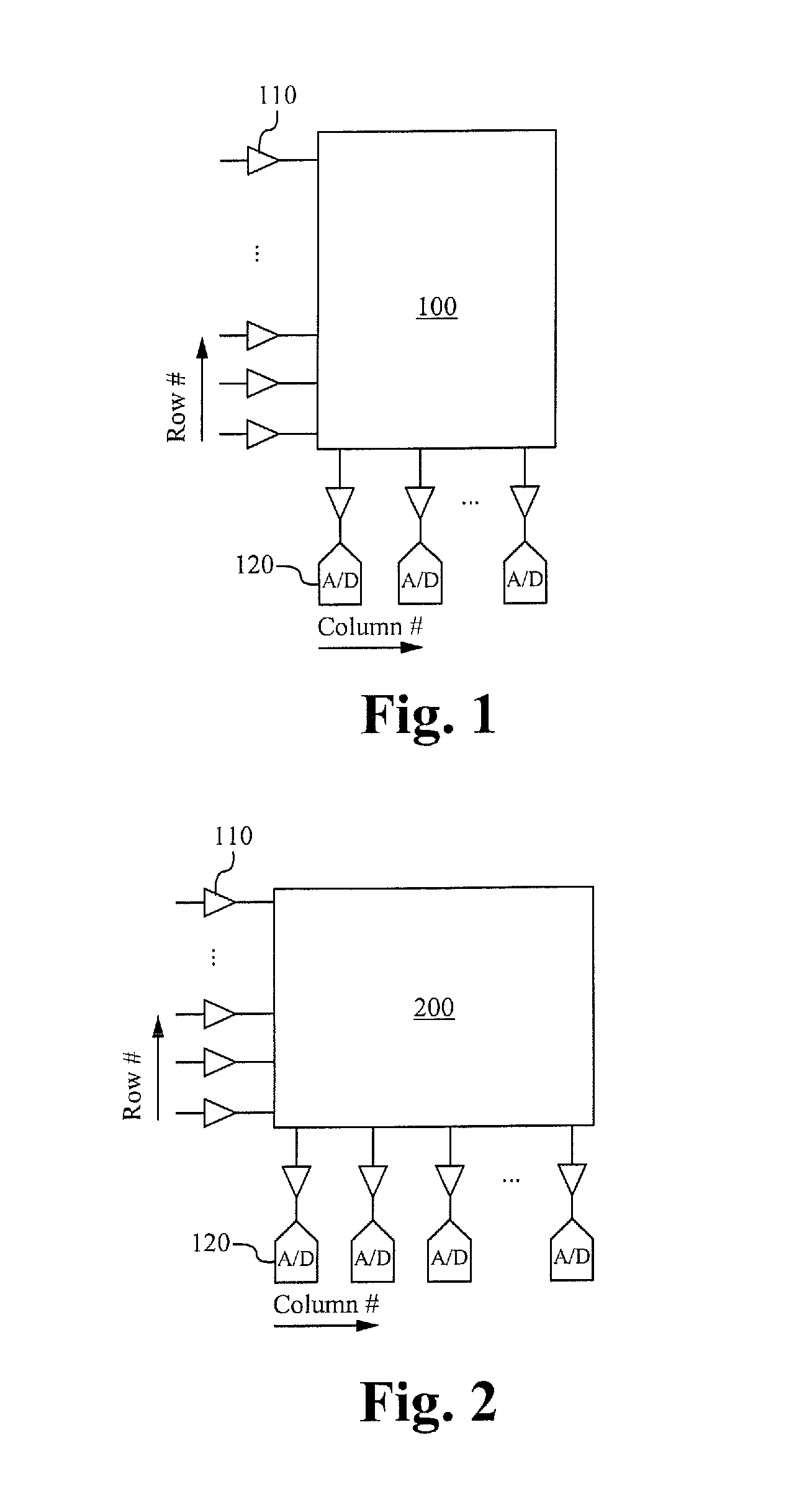
[0018]The present invention obviates the need to rotate large panels by 90 degrees for phase shift mitigation. As a result, the present invention allows the usage of the preferred configuration where there are many more row driver amplifiers than column A / Ds, which reduces the die area and power consumption of touch controller integrated circuits significantly. By using the innovative digital signal processing methodology of the present invention, the touch screen system is able to cope with extremely large phase shifts over the columns
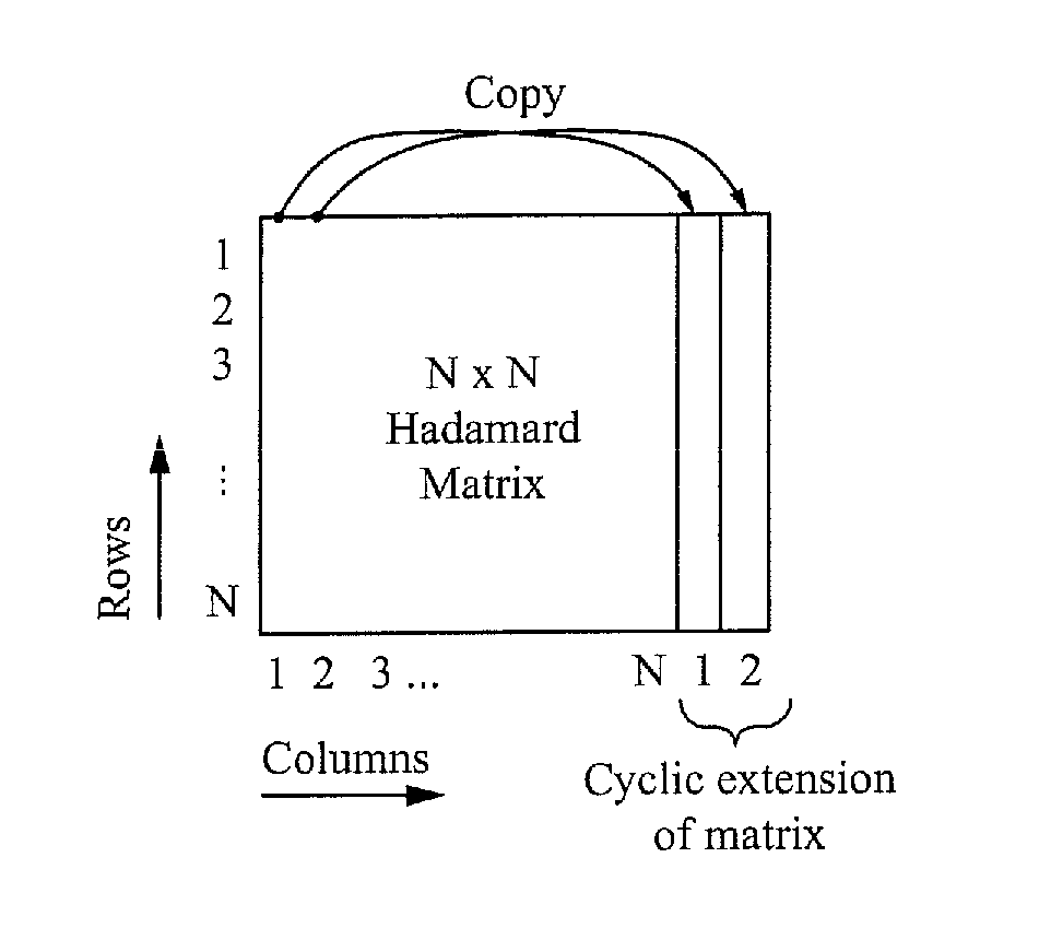
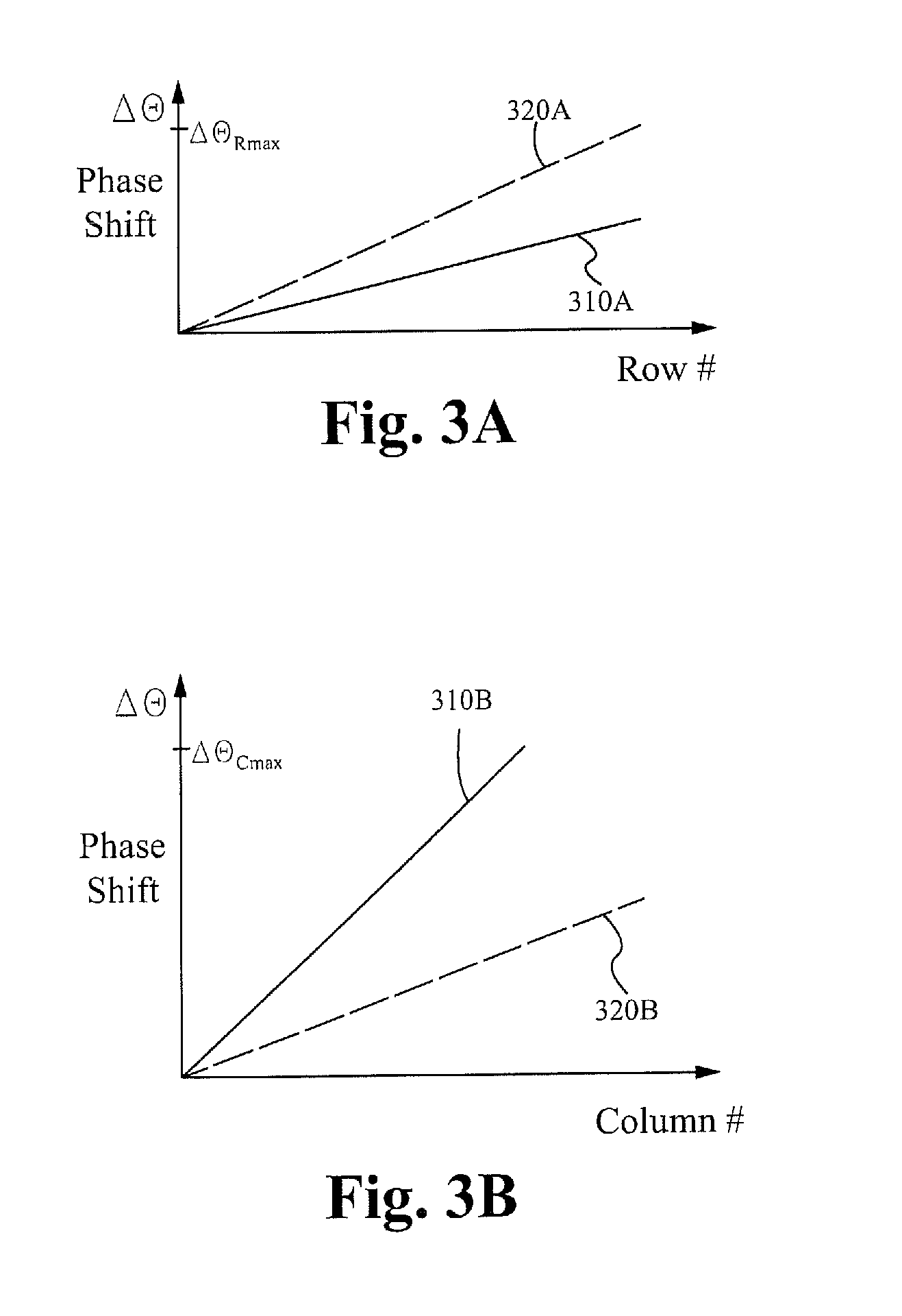
[0019]For high-speed baseband signaling, the present invention mitigates the problems discussed above by using orthogonal-based row signaling with a cyclical extension of the excitation matrix in the time dimension in order to maintain full relative orthogonality of each of the row drive signals, independent of the panel phase shift. In some embodiments, the orthogonal-based signaling involves the use of a Hadamard matrix as the excitation matrix. In some embodiments, the present invention uses a modified Hadamard matrix that is the dot product of a Hadamard matrix with a cover code matrix. The present invention also includes clustering a large panel into phase shift regions for digitally de-correlating and decoding signals. These features improve the panel signal processing and help ensure immunity to panel phase shifts, thereby enabling usage of large touch screen panels that have excessive phase shifts that cannot be handled by the prior art due to unacceptable levels of ICI, while avoiding the 90-degree rotation of the large panel and the increase in power consumption and die area associated with it.

Problems solved by technology

Since the human body is an electrical conductor, when a finger actuates the touch screen, such as by touching or even getting very close to its surface, the electrostatic field of the touch screen is distorted, resulting in a measurable change in capacitance.
Additionally, the condition number of the excitation matrix is important, since a high condition number will result in the amplification of errors and a less perfect estimation of the capacitance values.
Unfortunately, since there are more columns than rows in the rotated configuration, more A / Ds and low-noise amplifiers (LNAs) are being used, which results in the touch controller chip being more expensive, as well as a significant increase in power consumption and silicon die area.
These misalignments or time shifts produce bleeding of touch data of column pixels into each other, and therefore result in an increase in the artificial noise floor, not related to thermal and quantization noise, but related to intersymbol interference (ISI).
The use of a non-orthogonal matrix results in a large inter-code interference (ICI) with a relative shift between rows.
As a result, a non-orthogonal matrix produces a poor S / N for large panels.
Another impact of the phase shift over the column is that the sum of rows for each column is no longer constant, and can become very large for a large panel.
As a result, the DC cancellation is not effective, and the dynamic range of the A / Ds has to be increased by several bits.

Method used


Image

  • Mutual capacitance large panel phase shift mitigation
  • Mutual capacitance large panel phase shift mitigation
  • Mutual capacitance large panel phase shift mitigation

Examples


Embodiment Construction

[0052]The following description is presented to enable one of ordinary skill in the art to make and use the invention and is provided in the context of a patent application and its requirements. Various modifications to the described embodiments will be readily apparent to those skilled in the art and the generic principles herein can be applied to other embodiments. Thus, the present invention is not intended to be limited to the embodiment shown but is to be accorded the widest scope consistent with the principles and features described herein.

[0053]The present invention can be provided as a computer program product that can include a machine-readable medium having stored thereon instructions that can be used to program a computer (or other electronic devices) to perform a process according to the present invention. The machine-readable medium can include, but is not limited to, floppy diskettes, optical disks, CD-ROMs, ROMs, RAMs, magnet or optical cards, or other type of media / m...


PUM


Abstract

A method of mitigating a phase shift in a mutual capacitance touch screen panel having a plurality of row conductors intersecting with a plurality of column conductors to form a matrix of pixels, the method comprising: driving the row conductors with row drive signals formed from an excitation matrix, wherein each row in the excitation matrix is orthogonal to every other row in the excitation matrix, and the excitation matrix has a dimension larger than the matrix of pixels; sensing signals from the column conductors; and determining the mutual capacitance of the pixels using the sensed signals and an inverse of the excitation matrix. The excitation matrix can be a Hadamard matrix or a modified Hadamard matrix and can comprise a cyclic extension at the end of each row. A different region-specific phase shift can be applied to different clusters of signals.

Description

FIELD OF THE INVENTION[0001]The present invention relates to the field of touch screens. More specifically, the present invention relates to phase shift mitigation for touch screens.BACKGROUND OF THE INVENTION[0002]Many modern electronic devices incorporate a touch screen to display information and as an input that is activated by touching the display. One technology for implementing the touch aspect of a touch screen is capacitance sensing. An insulator, such as glass, is coated with a transparent conductor, such as indium tin oxide (ITO). Since the human body is an electrical conductor, when a finger actuates the touch screen, such as by touching or even getting very close to its surface, the electrostatic field of the touch screen is distorted, resulting in a measurable change in capacitance.[0003]A mutual capacitance touch screen comprises two layers of material arranged in an X-Y grid such that an actuation of the touch screen can be resolved into a coordinate. A finger is typi...

Claims


Application Information

Patent Timeline
Patent Type & Authority Patents(United States)
IPC IPC(8): G06F3/045G06F3/041G06F3/044
CPCG06F3/041G06F3/044G06F3/045G06F3/0446G06F3/04166
Inventor MOHINDRA, RISHI
Owner QUALCOMM INC
Why Eureka
Try Eureka