Sensor device

a sensor and sensor technology, applied in the field of sensor devices, can solve the problems of low accuracy, noise generation, difficult to respond to high-speed operation, etc., and achieve the effects of short signal processing steps, high-speed response, and simple circuit configuration

Active Publication Date: 2016-02-16
ABLIC INC
View PDF5 Cites 1 Cited by
  • Summary
  • Abstract
  • Description
  • Claims
  • Application Information

AI Technical Summary

Benefits of technology

[0029]The present invention has been made in view of the above-mentioned circumstances, and it is an object thereof to provide a magnetic sensor device capable of removing the influence of offset voltages of a magnetoelectric conversion element and input offset voltages of an amplifier and a comparator by a simple circuit configuration and detecting magnetic field intensity with high precision at high speed.
[0032]According to the sensor device of the exemplary embodiment of the present invention, the switch, the capacitor, and the amplifier having a plurality of differential input pairs are made use of effectively so that offset components generated in the sensor element, the differential amplifier, and the amplifier of the sensor device may be removed by a simple circuit configuration. Further, a signal processing step is shortened and its operating timings are appropriately set, and hence the detection following a high-speed change in magnetic field may be performed with minimal addition of circuits. Therefore, a sensor device capable of highly-precise and high-speed response may be provided.

Problems solved by technology

In general, the output voltage of the magnetoelectric conversion element is minute, and hence an error may occur due to an offset voltage of the magnetoelectric conversion element (element offset voltage), an offset voltage of the amplifier or the comparator (input offset voltage), and noise of those components, and the accuracy may be lower.
The noise is generated mainly by flicker noise of a single transistor of the circuit or thermal noise of a single transistor or a resistive element.
In the conventional magnetic sensor device described above, one period of the detection operation is made up of three phases, and hence it has been difficult to respond to high-speed operation.
The circuit area becomes larger with an increase in current consumption of the differential amplifier in particular.

Method used


Image

  • Sensor device
  • Sensor device
  • Sensor device

Examples


first embodiment

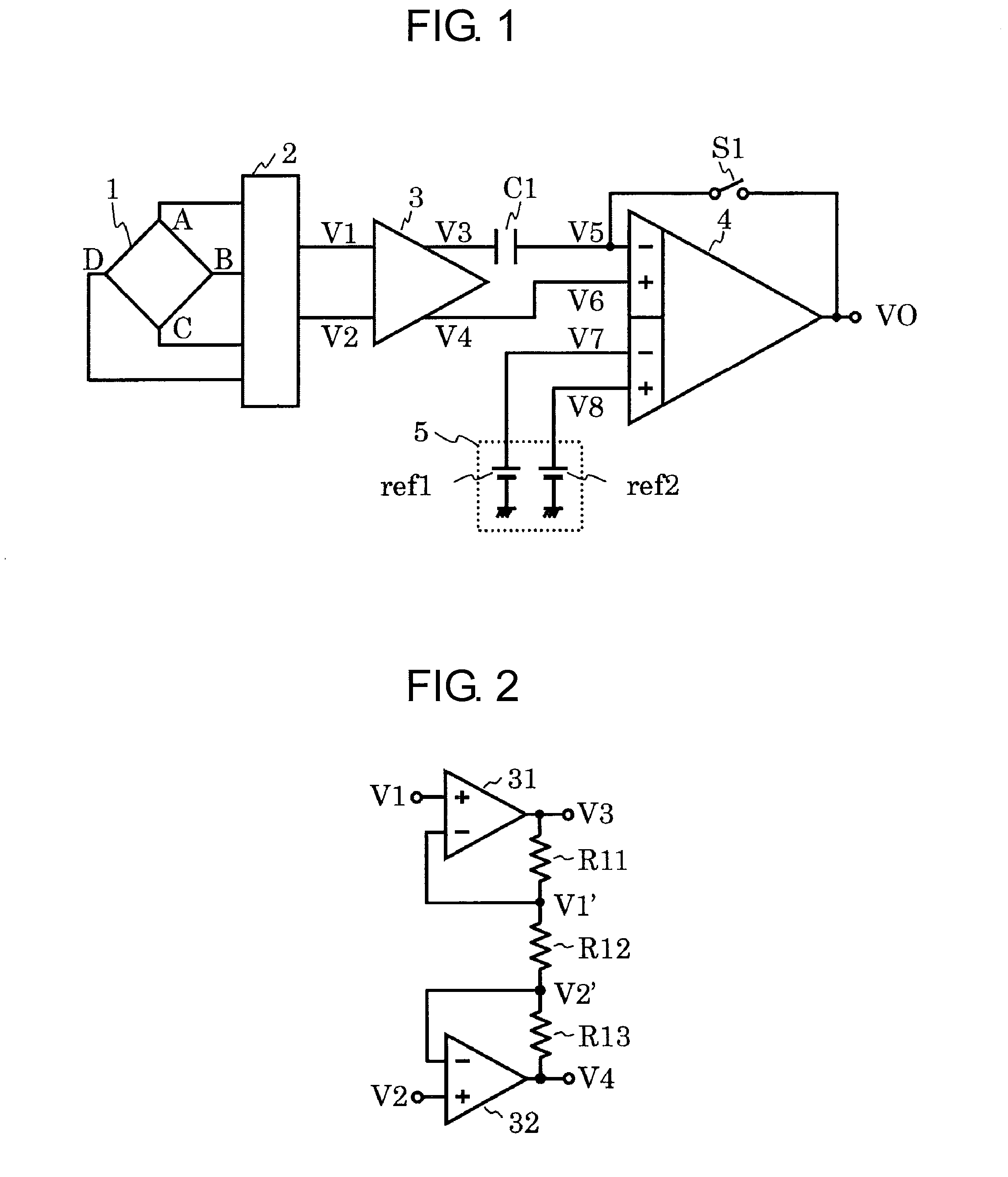
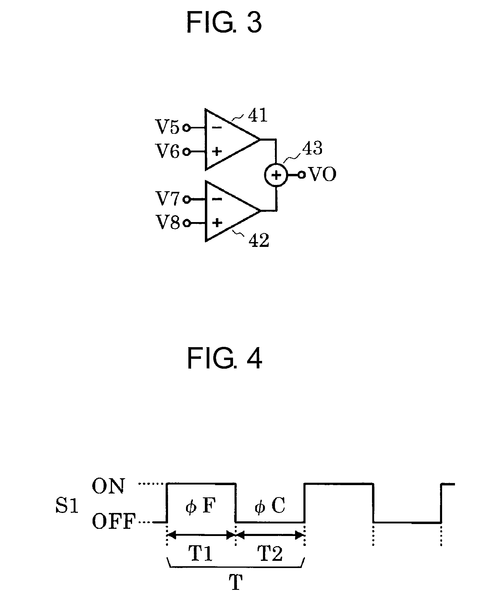
[0059]FIG. 1 is a circuit diagram of a magnetic sensor device according to a first embodiment of the present invention. The magnetic sensor device in the first embodiment includes a Hall element 1 serving as a magnetoelectric conversion element, a switch circuit 2, a differential amplifier 3, an amplifier 4, a capacitor C1, a switch S1, and a detection voltage setting circuit 5. The detection voltage setting circuit 5 includes a reference voltage circuit ref1 and a reference voltage circuit ref2.

[0060]The Hall element 1 includes a first terminal pair A-C and a second terminal pair B-D.

[0061]The switch circuit 2 includes four input terminals connected to the terminals A, B, C, and D of the Hall element 1, respectively, a first output terminal, and a second output terminal.

[0062]The differential amplifier 3 has a first input terminal V1, a second input terminal V2, a first output terminal V3, and a second output terminal V4. The first input terminal V1 and the second input terminal V2...

second embodiment

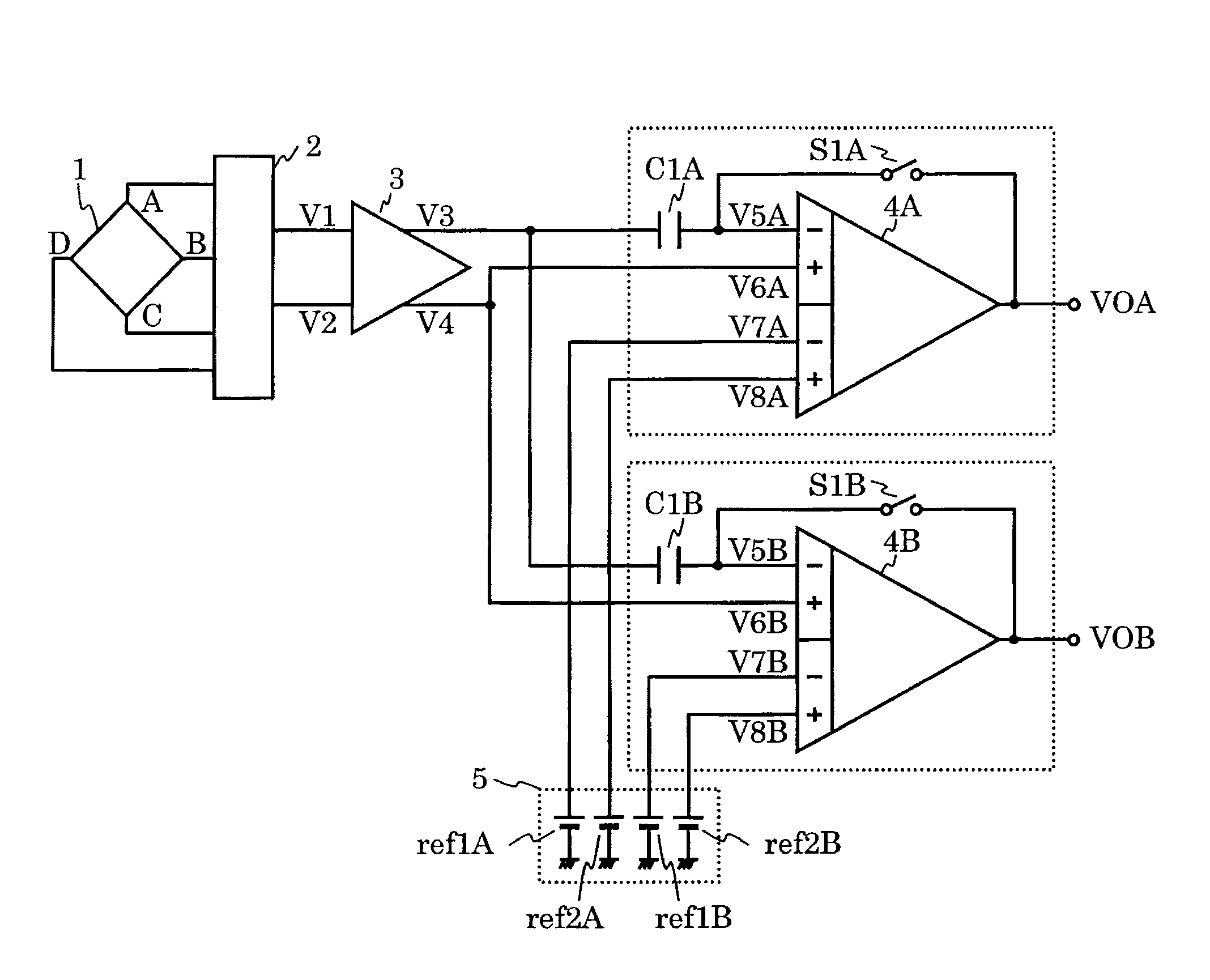
[0158]FIG. 12 is a circuit diagram of a magnetic sensor device according to a second embodiment of the present invention. The second embodiment of FIG. 12 is different from the first embodiment of FIG. 1 in that an amplifier 4B, a capacitor C1B, and a switch S1B are added and symbol A is suffixed to the amplifier 4, the capacitor C1, and the switch S1 for clear discrimination from the added components, and that a reference voltage circuit ref1B and a reference voltage circuit ref2B are added in the detection voltage setting circuit 5 and symbol A is suffixed to the reference voltage circuit ref1 and the reference voltage circuit ref2 for clear discrimination from the added components. Symbols A and B are suffixed also to the terminals for discrimination. The added components are configured and connected as follows.

[0159]Similarly to the configuration of the capacitor C1A, the capacitor C1B has two terminals. One terminal is connected to the first output terminal V3 of the differenti...

third embodiment

[0205]FIG. 20 is a circuit diagram of a magnetic sensor device according to a third embodiment of the present invention. The third embodiment of FIG. 20 is different from the first embodiment of FIG. 1 in that a capacitor C2 and a switch S2 are added, and that a reference voltage circuit ref0 is added in the detection voltage setting circuit 5. The added components are configured and connected as follows.

[0206]The capacitor C2 has two terminals. One terminal is connected to the second output terminal V4 of the differential amplifier 3. The other terminal is connected to the second input terminal V6 of the first differential input pair of the amplifier 4.

[0207]The switch S2 has two terminals. One terminal is connected to the second input terminal V6 of the first differential input pair of the amplifier 4. The other terminal is connected to a positive terminal of the reference voltage circuit ref0. The switch S2 is controlled to be turned ON or OFF in accordance with a switch control ...


PUM

PropertyMeasurementUnit
reference voltageaaaaaaaaaa
voltageaaaaaaaaaa
voltagesaaaaaaaaaa

Abstract

Provided is a sensor device capable of removing the influence of each offset voltage of a sensor element, a differential amplifier, and an amplifier of the sensor device, to thereby detect a physical quantity with high precision and respond to high-speed operation. The sensor device includes: a switch circuit connected to a first terminal pair and a second terminal pair of the sensor element, for controlling switching of the terminal pairs and outputting signal voltages; a differential amplifier including a first input terminal and a second input terminal connected to a first output terminal and a second output terminal of the switch circuit, respectively, for outputting a result obtained by amplifying a difference of the signal voltages; an amplifier including at least two differential input pairs, one of which inputs the differential signal output from the differential amplifier, and at least one of which inputs a reference signal corresponding to a physical quantity to be detected; and a detection voltage setting circuit for outputting the reference signal to the amplifier. Switching of the switch circuit provides a first detection state and a second detection state, and detection is performed in one first detection state and one second detection state.

Description

RELATED APPLICATIONS[0001]This application is a continuation of PCT / JP2013 / 060883 filed on Apr. 11, 2013, which claims priority to Japanese Application Nos. 2012-103219 filed on Apr. 27, 2012 and 2013-025969 filed on Feb. 13, 2013. The entire contents of these applications are incorporated herein by reference.BACKGROUND OF THE INVENTION[0002]1. Field of the Invention[0003]The present invention relates to a sensor device for detecting a physical quantity and converting the detected physical quantity such as magnetic field intensity into an electric signal.[0004]2. Description of the Related Art[0005]A magnetic sensor device is used as a sensor for detecting an open / close state in a flip mobile phone, a notebook computer, or the like and as a sensor for detecting a rotary position of a motor or the like (see, for example, Japanese Patent Application Laid-open No. 2010-281801).[0006]FIG. 18 illustrates a circuit diagram of a conventional magnetic sensor device. In the conventional magn...

Claims


Application Information

Patent Timeline
Patent Type & Authority Patents(United States)
IPC IPC(8): G01R17/02G01R33/02G01L1/00G01R33/07G01R33/00
CPCG01R33/07G01R33/0023G01L1/00G01R33/0029G01R33/02
Inventor ARIYAMA, MINORUMURAOKA, DAISUKEHIKICHI, TOMOKIFUKAI, KENTARO
Owner ABLIC INC
Why Eureka
Try Eureka