Etching method and apparatus

a silicon oxide film and etching method technology, applied in the direction of electrical equipment, basic electric elements, electric discharge tubes, etc., to achieve the effect of increasing the selectivity increasing the etching rate of silicon oxide films, and increasing the amount of carbon and fluorine in plasma

Active Publication Date: 2016-02-16
TOKYO ELECTRON LTD
View PDF14 Cites 1 Cited by
  • Summary
  • Abstract
  • Description
  • Claims
  • Application Information

AI Technical Summary

Benefits of technology

[0009]In view of the above, the present invention provides a novel etching method and apparatus capable of increasing selectivity of a silicon oxide film with respect to a silicon nitride film.
[0012]When the flow rate ratio of the CHF-based gas to the plasma excitation gas is increased to 1 / 15 or higher, the amount of carbon and the amount of fluorine in the plasma increase. Since the amount of fluorine contributing to etching increases, it is possible to increase the etching rate of the silicon oxide film. Meanwhile, since the surface of the silicon nitride film is more chemically unstable than the surface of the silicon oxide film, carbon-based deposits are deposited on the surface of the silicon nitride film. Thus, even if the amount of fluorine contributing to etching increases, the etching rate of the silicon nitride film does not increase as much as that of the silicon oxide film. Therefore, it is possible to increase the selectivity of the silicon oxide film with respect to the silicon nitride film.
[0013]Further, by using a CHF-based gas as an etching gas, it is possible to control the etching rates of the silicon oxide film and the silicon nitride film.

Problems solved by technology

Meanwhile, since the surface of the silicon nitride film is more chemically unstable than the surface of the silicon oxide film, carbon-based deposits are deposited on the surface of the silicon nitride film.

Method used


Image

  • Etching method and apparatus
  • Etching method and apparatus
  • Etching method and apparatus

Examples


Embodiment Construction

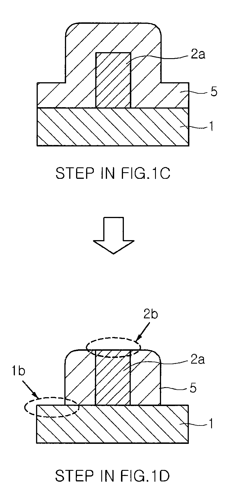
[0021]Hereinafter, an etching method in accordance with a first embodiment of the present invention will be described with reference to the accompanying drawings. Throughout the drawings, the same reference numerals are given to the same components.

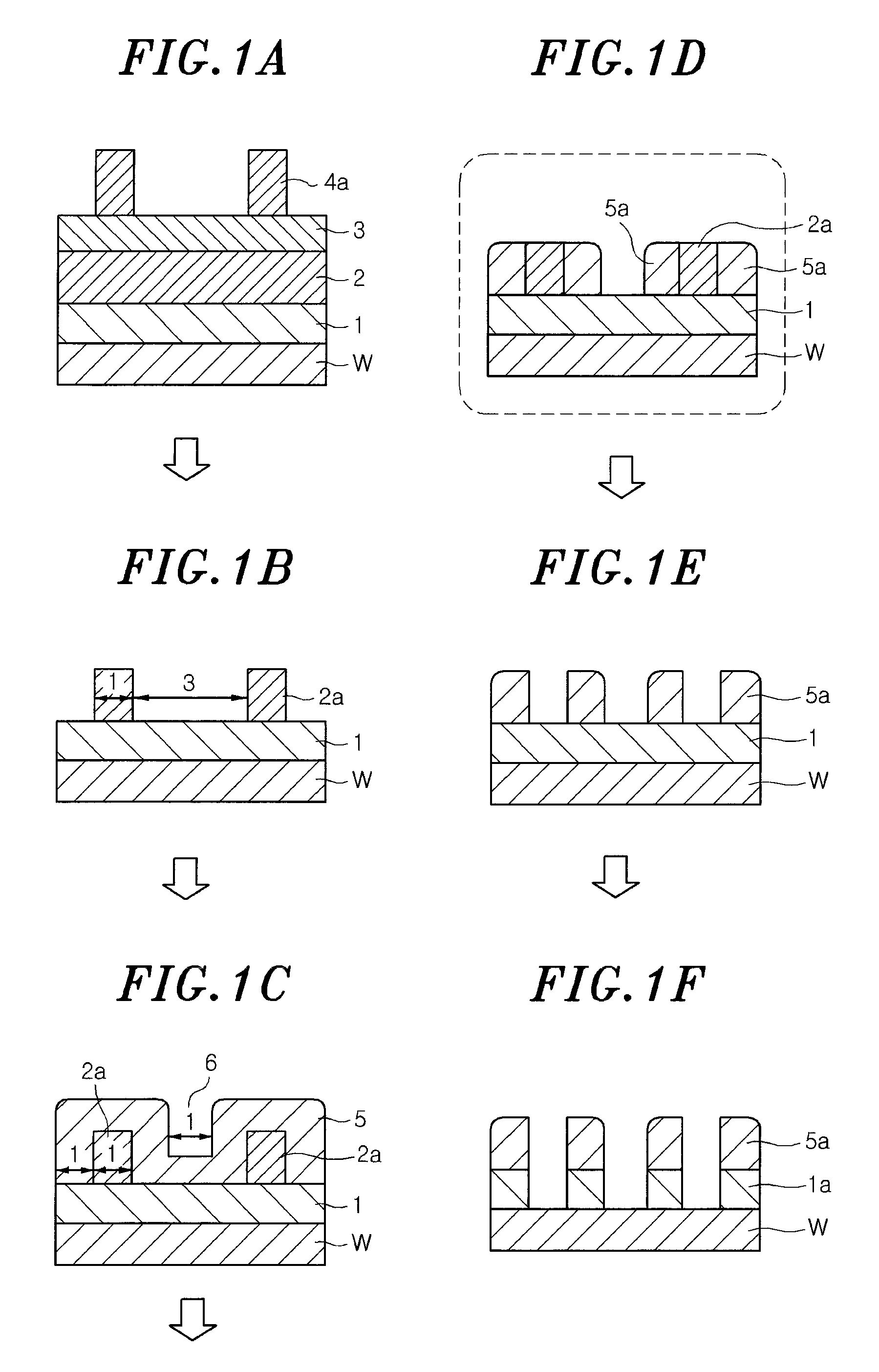
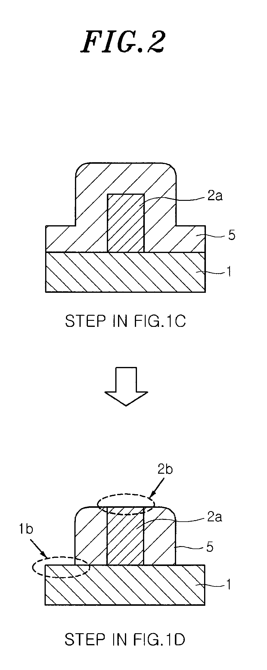
[0022]The steps of double patterning to which the etching method of the first embodiment is applied are shown in FIGS. 1A to 1F.

[0023]As shown in FIG. 1A, a silicon nitride film 1, a polysilicon film 2 and a bottom anti-reflection coating (BARC) film 3 are sequentially stacked on a wafer (substrate) W made of silicon or the like. The silicon nitride film 1 and the polysilicon film 2 are formed by, e.g., a chemical vapor deposition (CVD) method. An ArF photoresist is coated on a surface of the BARC film 3. A mask pattern is transferred to the photoresist layer by exposure. The exposed photoresist layer is developed. After development, resist patterns 4a are formed on the upper surface of the BARC film 3. The resist patterns 4a include, e.g...


PUM

PropertyMeasurementUnit
binding energyaaaaaaaaaa
depthaaaaaaaaaa

Abstract

An etching method and apparatus for etching a silicon oxide film selectively with respect to a silicon nitride film formed on a substrate are provided. A processing gas containing a plasma excitation gas and a CHF-based gas is introduced into a processing chamber such that a flow rate ratio of the CHF-based gas to the plasma excitation gas is 1 / 15 or higher. By generating a plasma in the processing chamber, the silicon oxide film is etched selectively with respect to the silicon nitride film formed on the substrate in the processing chamber.

Description

CROSS REFERENCE TO RELATED APPLICATIONS[0001]This application is a Continuation application of PCT International Application No. PCT / JP2012 / 074468 filed on Sep. 25, 2012, which designated the United States, which claims priority to and the benefit of Japanese Patent Application No. 2011-212450 filed Sep. 28, 2011, the disclosures of which are incorporated herein by reference in their entireties.FIELD OF THE INVENTION[0002]The present invention relates to a method and apparatus for selectively etching a silicon oxide film with respect to a silicon nitride film formed on a substrate.BACKGROUND OF THE INVENTION[0003]Semiconductor integrated circuits have been developed to have high performance and high integration in response to miniaturization of devices. In recent years, miniaturization is being advanced in the device design rules, but optical lithography that is a main technique of miniaturization is approaching the practical limit.[0004]In order to obtain highly miniaturized patter...

Claims


Application Information

Patent Timeline
Patent Type & Authority Patents(United States)
IPC IPC(8): H01J37/32H01L21/302H01L21/461H01L21/3065H01L21/311H01L21/67H01L21/33H01L21/033
CPCH01L21/3065H01J37/3222H01J37/3244H01J37/32192H01L21/0337H01L21/31116H01L21/31144H01L21/67069
Inventor SEKINE, TAKAYUKISASAKI, MASARUMATSUMOTO, NAOKISHINPUKU, EIICHIROU
Owner TOKYO ELECTRON LTD
Why Eureka
Try Eureka