Electronic device

a technology of electronic devices and electronic components, applied in semiconductor devices, diodes, capacitors, etc., can solve the problems of increasing requiring cryogenic operation temperatures or slow switching frequency, and not being able to accept the on/off ratio of respective active devices

Inactive Publication Date: 2016-02-23
FRIEDRICH ALEXANDER UNIV ERLANGEN NURNBERG
View PDF6 Cites 0 Cited by
  • Summary
  • Abstract
  • Description
  • Claims
  • Application Information

AI Technical Summary

Benefits of technology

[0036]Preferably the electronic device comprises a resistor element, which is constructed by at least one strip of the at least one first or second electrode. The resistance of such a graphene strip is calculated from the known resistance of the graphene layer and the given length or geometry of the strip. One additional advantage of the invention in that context is that there is no contact resistance at a contact-gate-graphene junction. Therefore, gate graphene and contact graphene may be connected to each other without considering electric transport properties of a junction of both graphene types. Alternatively or additionally the resistance of the conductive layer within the substrate is used. To yield a defined resistance of the conductive layer the current path for example is spatially narrowed by a second electrode having a gate graphene layer or by a appropriate lateral doping profile.
[0037]In a preferred embodiment of the invention, the resistor strip has a meandering pattern. This allows a packed construction of the resistor element.
[0038]According to another embodiment of the invention the first electrode is substantially surrounded by the second electrode. The surrounding second electrode confines the current paths to and from the first electrode through the conductive layer of the substrate. A ring shaped second electrode for example is preferred when all possible current paths to and from the first electrode should be narrowed down in an off state of the device. The surrounding second electrode is also used to align the current flow within the conductive layer of the substrate.
[0039]Advantageously the electronic device comprises at least one conductor strip, which is formed by a second electrode strip or by a first electrode strip which is surrounded by a second electrode strip. Both embodiments avoid leakage currents through the substrate when connecting the graphene electrodes to said conductor strips electrically. Alternatively other metal strips may be used for the electrical connection of the graphene layers.
[0040]According to another preferred embodiment of the invention, the electronic device is an integrated circuit, wherein a plurality of first and second electrodes is comprised, at least two of these electrodes being electrically connected by a current path through the substrate.

Problems solved by technology

Due to the lack of a sufficiently large band gap, gating the graphene will therefore not result in an acceptable on / off-ratio of respective active devices.
The on / off-ratio is increased when using a thin graphene strip or by chemical modification of the graphene layers, where both methods result in disadvantages like the requirement of cryogenic operation temperatures or slow switching frequencies.
The Schottky barrier of a gate graphene layer disposed on the surface is not able to stop a horizontal current flow through the conductive layer.

Method used


Image

  • Electronic device
  • Electronic device
  • Electronic device

Examples


Embodiment Construction

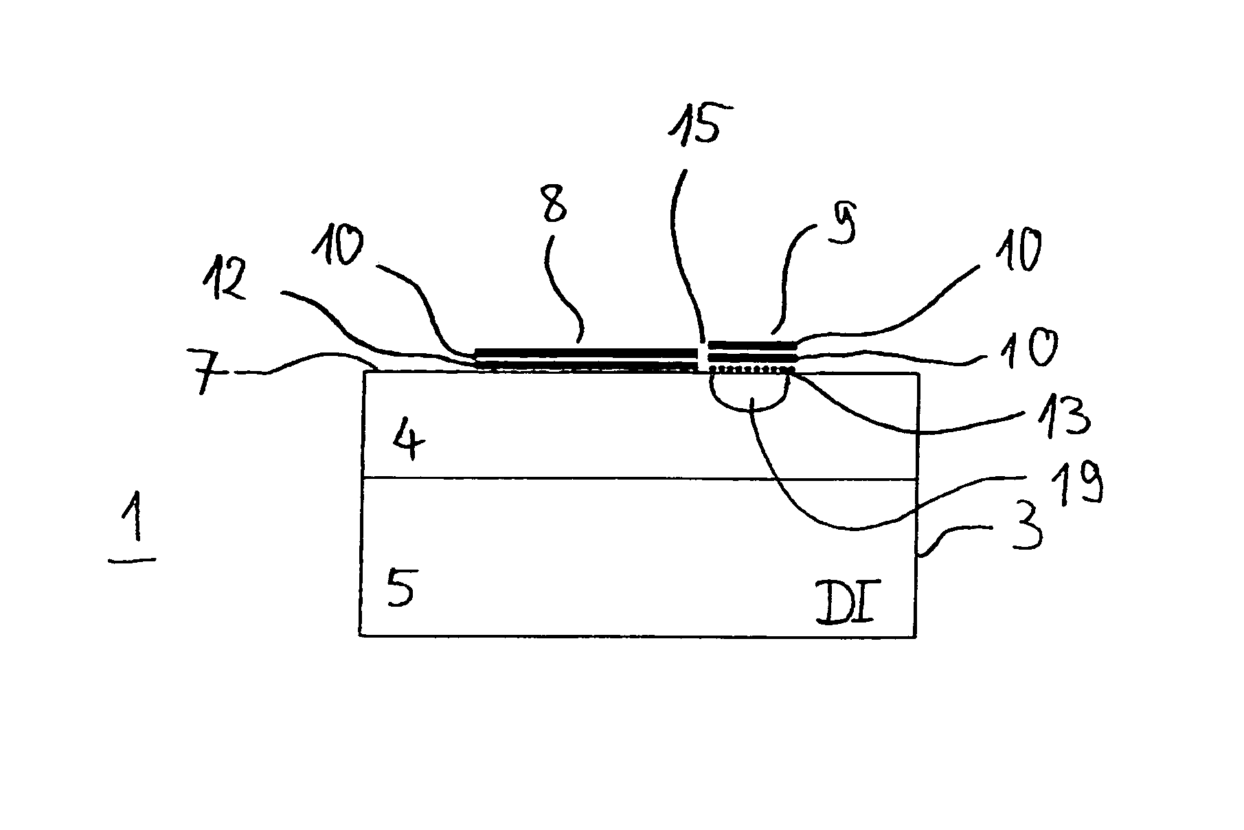
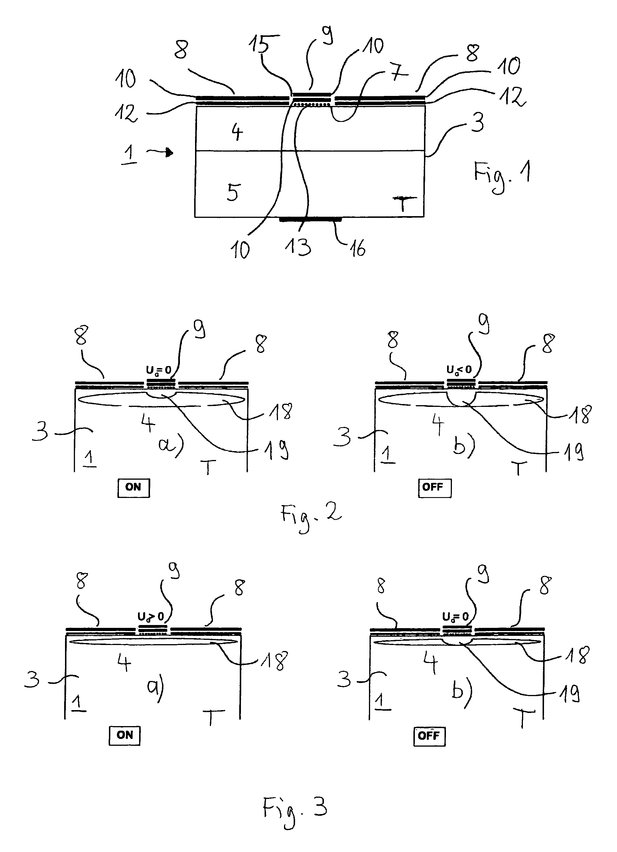
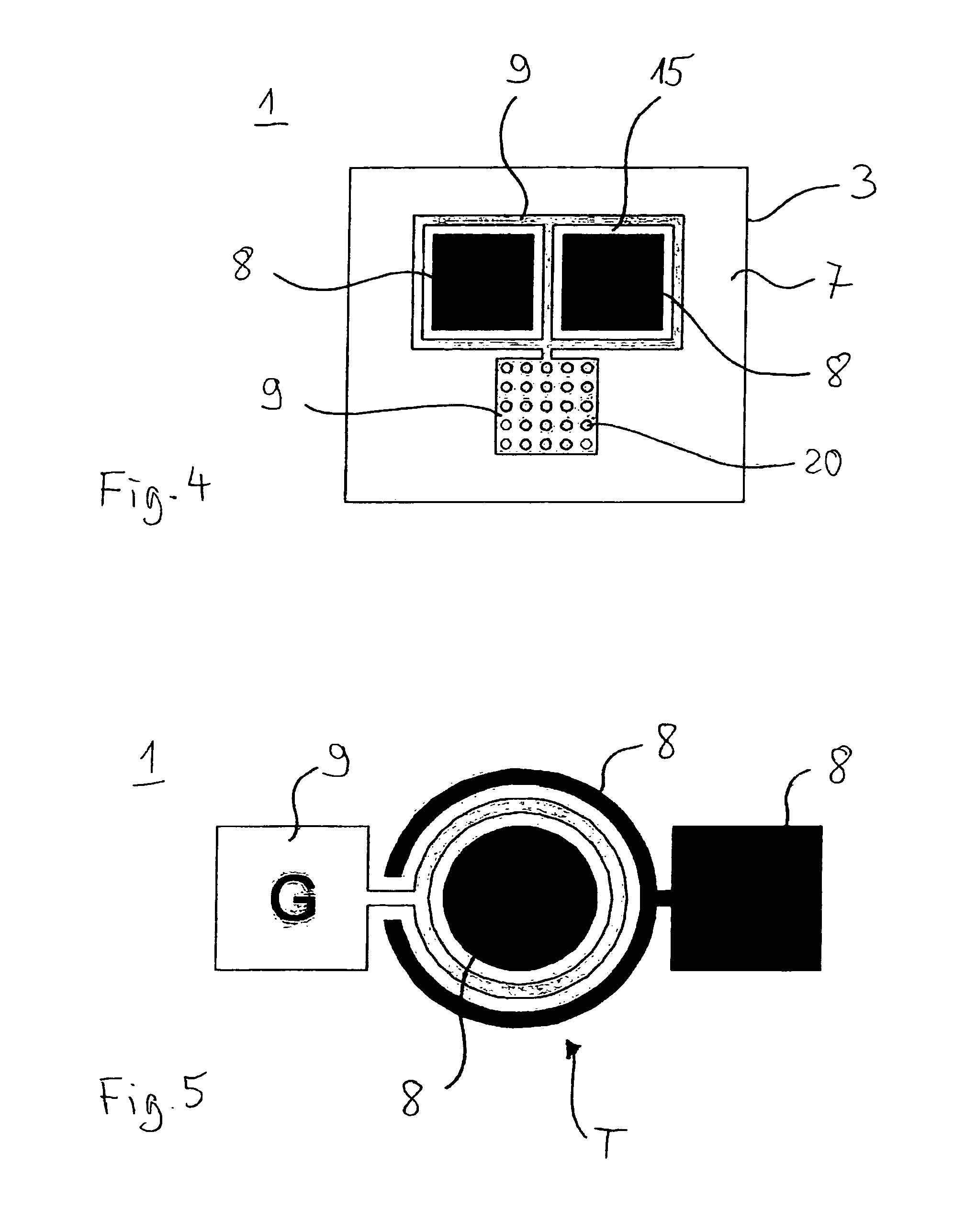
[0054]FIGS. 1-3 are schematic cross-sectional views of electronic devices 1 having a semiconductor substrate 3. The semiconductor substrate 3 comprises a first zone 4, which is doped with n-type impurities, and a second zone 5, which is doped with p-type impurities. Only the first zone 4 of the substrate 3 is shown in FIGS. 2 and 3.

[0055]On the front surface 7 of the substrate 3 two first electrodes 8 and a second electrode 9 are disposed. The second electrode 9 is disposed between the two first electrodes 8. The first and the second electrodes 8, 9 each comprise at least one epitaxial graphene monolayer 10. The at least one epitaxial graphene monolayer 10 of the first electrodes 8 is forming an ohmic contact with the substrate 3. Between the epitaxial graphene monolayer 10 of the first electrode 8 and the surface 7 of the substrate 3 a carbon buffer layer 12 is exhibited. The at least one epitaxial graphene monolayer 10 of the second electrode 9 and the substrate 3 are forming a Sc...


PUM


Abstract

An electronic device (1) includes a semiconductor substrate (3) having a front surface (7), a first electrode (8) and a second electrode (9) disposed on the front surface (7) of the substrate (3), wherein the first electrode (8) and the second electrode (9) each have at least one epitaxial graphene monolayer (10). The at least one epitaxial graphene monolayer (10) of the first electrode (8) forms an ohmic contact with the substrate (3) and the at least one epitaxial graphene monolayer (10) of the second electrode (9) forms a Schottky barrier with the substrate (3).

Description

BACKGROUND[0001]1. Field of the Invention[0002]The present invention relates to an electronic device having a first electrode and a second electrode disposed on the front surface of a semiconductor substrate, wherein the first electrode and the second electrode each comprises at least one epitaxial graphene monolayer. More specifically, the invention relates to an integrated circuit with silicon carbide (SiC) as semiconductor substrate and graphene layers on that substrate.[0003]2. Description of the Related Art[0004]Monolithic integrated circuits are electronic circuits manufactured on one semiconductor substrate, comprising connected electronic devices like transistors, diodes, capacitors and resistors. Today, integrated circuits are mainly manufactured on the basis of Silicon (Si). However, other semiconductor materials may have advantages for specific application areas like high frequency or high power applications.[0005]Silicon carbide for example with a band gap of approximate...

Claims


Application Information

Patent Timeline
Patent Type & Authority Patents(United States)
IPC IPC(8): H01L29/49H01L27/12H01L21/84H01L29/812H01L29/872H01L29/66H01L29/47H01L29/45H01L29/423H01L29/417H01L49/02H01L27/06H01L21/82H01L29/16H01L21/04
CPCH01L29/1606H01L21/0485H01L21/0495H01L21/8213H01L21/84H01L27/0605H01L27/0629H01L27/1203H01L28/22H01L28/40H01L29/41758H01L29/42316H01L29/45H01L29/47H01L29/66143H01L29/812H01L29/872H01L29/1608
Inventor WEBER, HEIKO B.KRIEGER, MICHAELHERTEL, STEFANKRACH, FLORIANJOBST, JOHANNESWALDMANN, DANIEL
Owner FRIEDRICH ALEXANDER UNIV ERLANGEN NURNBERG
Why Eureka
Try Eureka