Memory device and semiconductor device
a memory device and semiconductor technology, applied in information storage, static storage, digital storage, etc., can solve the problems of getting finer, affecting the stability of data storage, so as to achieve the effect of reducing power consumption and reducing power consumption
- Summary
- Abstract
- Description
- Claims
- Application Information
AI Technical Summary
Benefits of technology
Problems solved by technology
Method used
Image
Examples
embodiment 1
(Embodiment 1)
1>
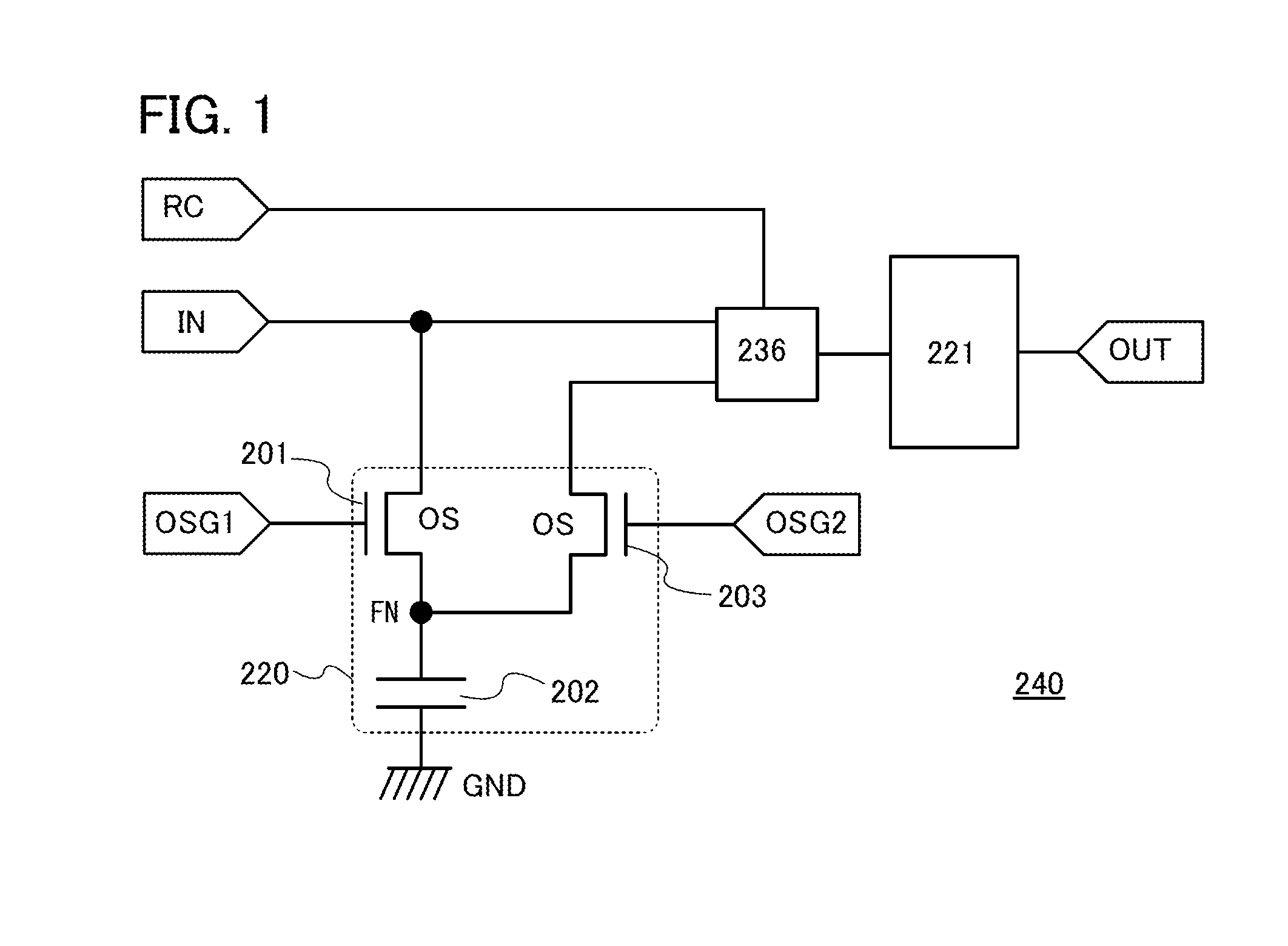
[0039]In Embodiment 1, the structure of a memory device of one embodiment of the present invention will be described with reference to FIG. 1.
[0040]A memory device 240 illustrated in FIG. 1 includes a memory circuit 220 including a first transistor 201, a second transistor 203, and a storage capacitor 202; a memory circuit 221 including a third transistor; and a selection circuit (also referred to as multiplexer) 236 including a fourth transistor.
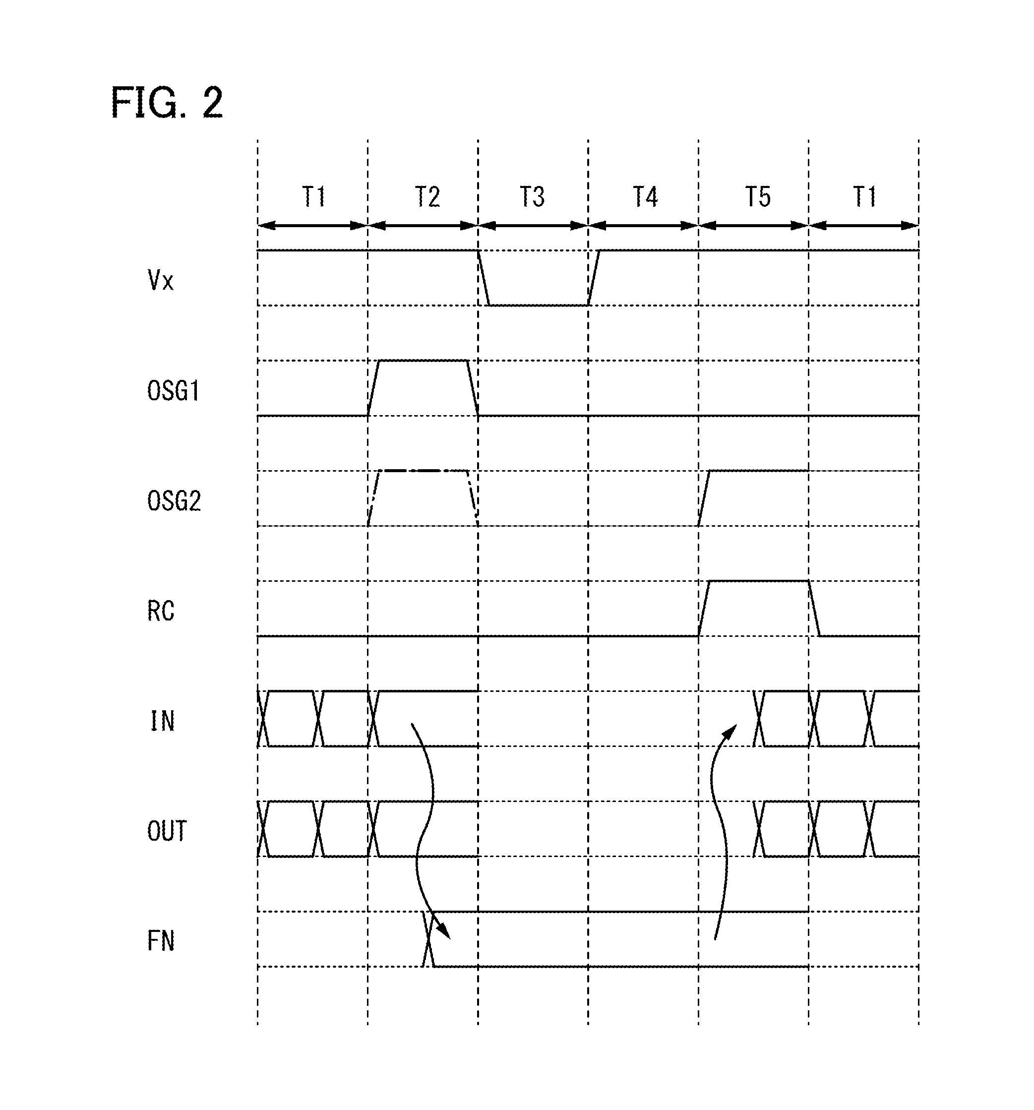
[0041]As the first transistor 201 and the second transistor 203, a transistor using an oxide semiconductor for a channel formation region (OS transistor) is used, for example. Because of their very low off leakage current, the OS transistors can form the memory circuit 220 in which a signal stored in the storage capacitor 202 can be held during power interruption. The memory circuit 220 including the OS transistors as the first transistor 201 and the second transistor 203 has the advantage of no performance degradation due t...
embodiment 2
(Embodiment 2)
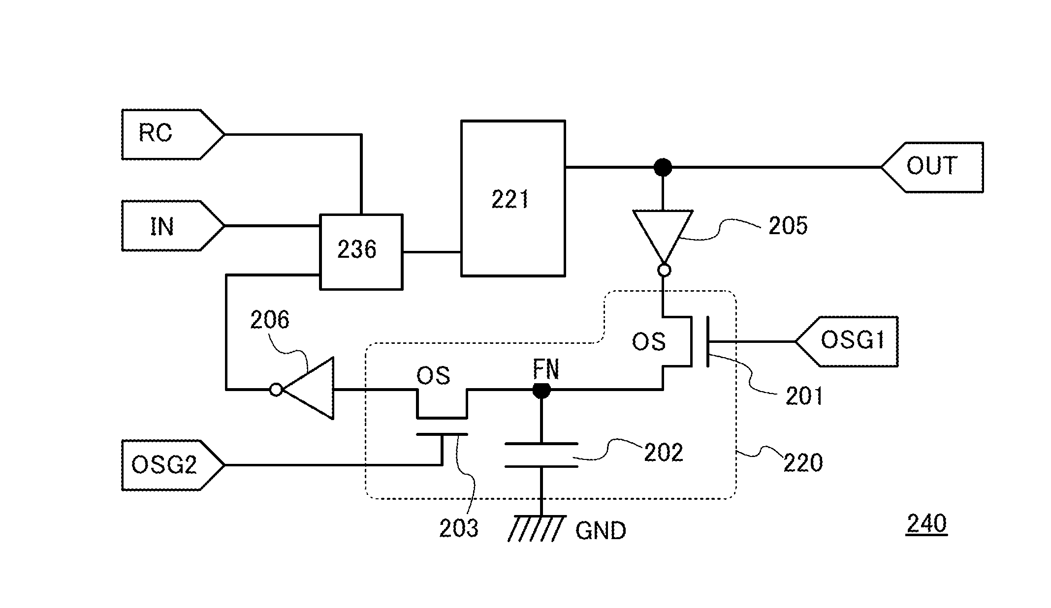
[0064]In Embodiment 2, the structures of a memory device of one embodiment of the present invention that are different from the structure of the memory device in FIG. 1 will be described with reference to FIGS. 3A and 3B.
[0065]FIG. 3A illustrates a structure where a buffer circuit 204 is provided between the other of the source and the drain of the second transistor 203 and the selection circuit 236. The other components are the same as in Embodiment 1. If the voltage of the input signal IN held in the storage capacitor 202 is lowered in the power supply voltage stop period, the loss of the voltage can be compensated owing to the buffer circuit 204 at the time of outputting the signal of the node FN and a proper voltage can be output as a result. When the loss of the voltage can be compensated by providing the buffer circuit 204, the guaranteed operating range of the memory device 240 can be expanded.
[0066]FIG. 3B illustrates a structure where an inverter circuit 205 i...
embodiment 3
(Embodiment 3)
[0068]In Embodiment 3, the structures of a memory device of one embodiment of the present invention that are different from those of the memory devices in FIG. 1 and FIGS. 3A and 3B will be described with reference to FIGS. 4A to 4C and FIGS. 5A to 5C.
[0069]In FIG. 4A, the other of the source and the drain of the first transistor 201 is electrically connected to the output terminal of the memory circuit 221. The other components are the same as in Embodiment 1. Note that the memory circuit 221 in FIG. 4A is configured so that a potential having the same level as the potential of the input signal IN input to the input terminal of the memory circuit 221 is output to the output terminal as the output signal OUT.
[0070]The storage capacitor 202 is connected to the first transistor 201 and the second transistor 203 but not directly connected to the gate of the third transistor or the fourth transistor. Accordingly, even if the gate leakage current of the third transistor or ...
PUM
 Abstract
Description
Claims
Application Information


