
Metallic contact for optoelectronic semiconductor device

a semiconductor device and contact technology, applied in the field of metal contacts, can solve the problems of high reflectivity or transparency, difficult formation of p-type ohmic contacts, low specific resistance, etc., and achieve the effect of increasing the overall reflectivity or transparency of contacts

Active Publication Date: 2016-04-12
SENSOR ELECTRONICS TECH
View PDF18 Cites 24 Cited by
  • Summary
  • Abstract
  • Description
  • Claims
  • Application Information

AI Technical Summary

Benefits of technology

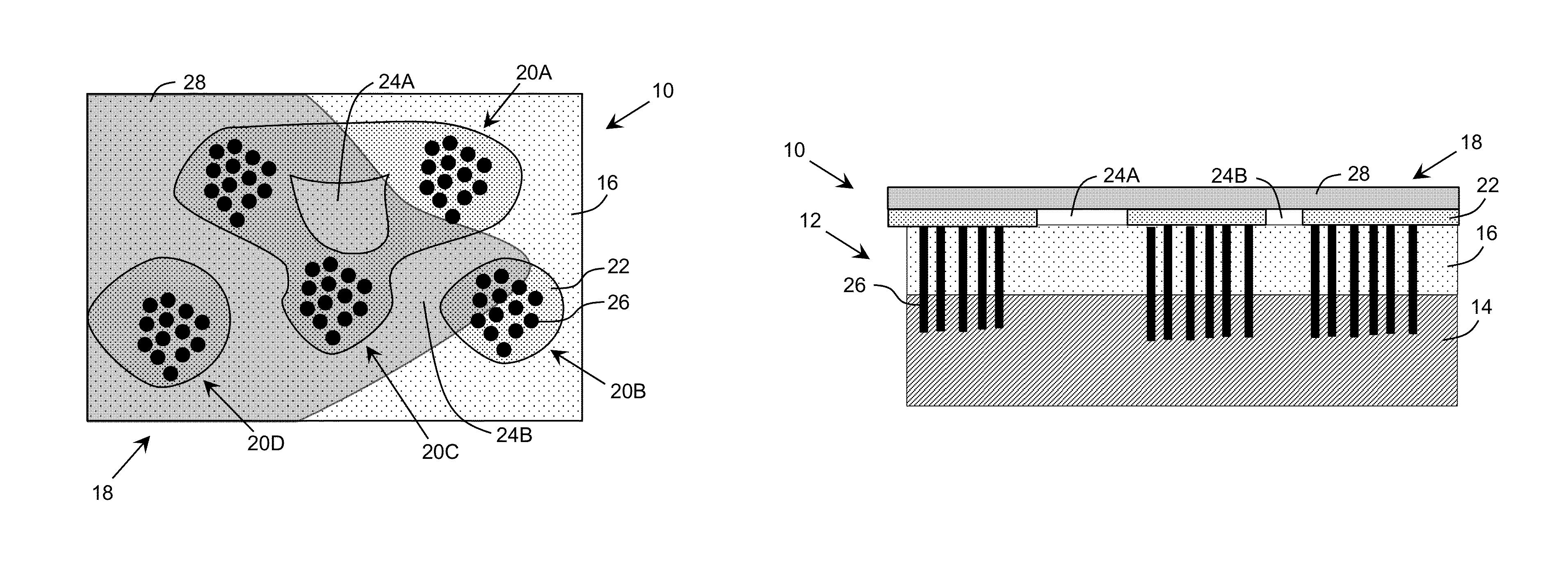
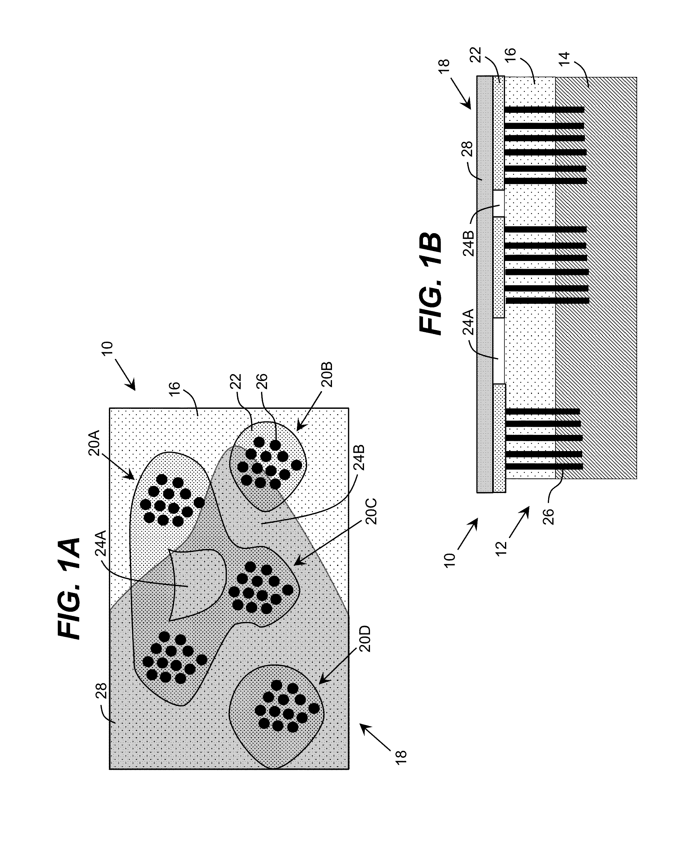
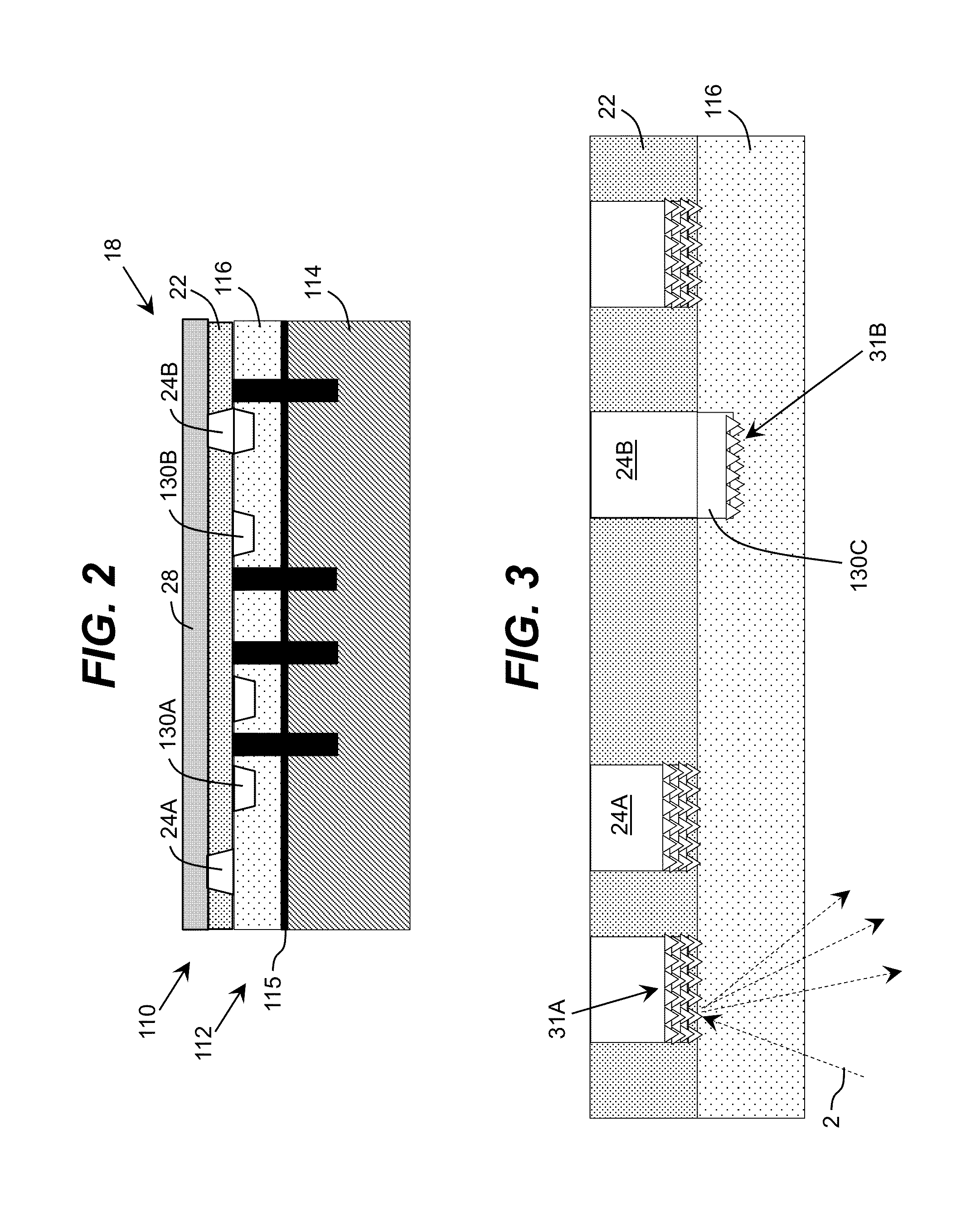
This patent describes a way to create a connection to a semiconductor layer in a light emitting structure. This connection has multiple metal areas separated by small empty spaces. These spaces are designed to increase the reflectivity or clarity of the connection.

Problems solved by technology

A challenge in developing optoelectronic semiconductor devices, such as light emitting diodes (LEDs), laser diodes (LDs), and photodiodes, is the development of an ohmic contact to n-type or p-type semiconductor layers, which has a low specific resistance while also having a high reflectivity or transparency.
Similarly, the challenge for manufacturing quality contacts to p-type nitride semiconductors is important for all nitride-based LEDs, since a relatively low p-doping (e.g., less than 1×1018 cm−3) in p-type GaN makes the formation of such p-type ohmic contacts difficult.
Developing a good ohmic contact is particularly challenging for semiconductor layers containing high levels of aluminum.
In particular, there are no metals that can match a high work function of p-doped AlGaN alloys.
The resulting difference between semiconductor and metal work functions results in formation of an Schottky barrier at the metal semiconductor junction.
A drawback of the recessed source and drain contacts is a presence of a short channel effect, which can deteriorate the device performance.
Making a p-type contact to p-type GaN, for example, is much more difficult.
In particular, it is difficult to grow well doped p-type GaN with a carrier concentration of more than 1018 cm−3 due to a high activation energy of acceptors.
Additionally, it is difficult to find metals with a work function that corresponds to p-type GaN.
In addition, use of superlattices, strained semiconductor layers, and spontaneous polarization have been employed to achieve a high hole concentration and result in a low contact resistivity.

Method used


Image

  • Metallic contact for optoelectronic semiconductor device
  • Metallic contact for optoelectronic semiconductor device
  • Metallic contact for optoelectronic semiconductor device

Examples


Embodiment Construction

[0041]As indicated above, aspects of the invention provide a metallic contact to a semiconductor layer in a light emitting structure. The contact can include a plurality of contact areas formed of a metal and separated by a set of voids. The contact areas can be separated from one another by a characteristic distance selected based on a set of attributes of a semiconductor contact structure of the contact and a characteristic contact length scale of the contact. The voids can be configured to increase an overall reflectivity or transparency of the contact. A metallic contact described herein can have a reduced Schottky barrier such that the nonlinear contact behavior can be ignored, which is referred to as an “ohmic contact” herein. As used herein, unless otherwise noted, the term “set” means one or more (i.e., at least one) and the phrase “any solution” means any now known or later developed solution.

[0042]Turning to the drawings, FIGS. 1A and 1B show top and lateral views, respect...


PUM


Abstract

A contact to a semiconductor layer in a light emitting structure is provided. The contact can include a plurality of contact areas formed of a metal and separated by a set of voids. The contact areas can be separated from one another by a characteristic distance selected based on a set of attributes of a semiconductor contact structure of the contact and a characteristic contact length scale of the contact. The voids can be configured to increase an overall reflectivity or transparency of the contact.

Description

REFERENCE TO RELATED APPLICATIONS[0001]The current application claims the benefit of U.S. Provisional Application No. 61 / 670,808, titled “Ohmic Contact for Optoelectronic Semiconductor Device,” which was filed on 12 Jul. 2012, and which is hereby incorporated by reference. Aspects of the invention are related to co-pending U.S. patent application Ser. No. 13 / 909,621, titled “Ohmic Contact to Semiconductor Layer,” which was filed on 4 Jun. 2013, and which is hereby incorporated by reference.TECHNICAL FIELD[0002]The disclosure relates generally to metallic contacts, and more particularly, to an improved method of manufacturing a metallic contact to a semiconductor layer.BACKGROUND ART[0003]A challenge in developing optoelectronic semiconductor devices, such as light emitting diodes (LEDs), laser diodes (LDs), and photodiodes, is the development of an ohmic contact to n-type or p-type semiconductor layers, which has a low specific resistance while also having a high reflectivity or tra...

Claims


Application Information

Patent Timeline
Patent Type & Authority Patents(United States)
IPC IPC(8): H01L33/38H01L33/60H01S5/32H01L33/40H01L33/42H01L33/36
CPCH01L33/382H01L33/40H01L33/42H01L33/60H01S5/32H01L33/387H01L33/36H01L33/38H01L33/405
Inventor LUNEV, ALEXANDERSHATALOV, MAXIM SDOBRINSKY, ALEXANDERSHUR, MICHAELGASKA, REMIGIJUS
Owner SENSOR ELECTRONICS TECH
Learn More