Check patentability & draft patents in minutes with Patsnap Eureka AI!

Thin low profile strip dual in-line memory module

a memory module and low-profile technology, applied in the direction of instruments, sustainable manufacturing/processing, semiconductor/solid-state device details, etc., can solve the problems of increasing the number of signal routing signals required for each memory chip on the dimm, increasing the cost of additional signaling lines, and increasing the difficulty of operation and cos

Active Publication Date: 2016-10-25
NXP USA INC
View PDF18 Cites 1 Cited by
  • Summary
  • Abstract
  • Description
  • Claims
  • Application Information

AI Technical Summary

Benefits of technology

This design achieves higher capacity density, lower power consumption, lower costs, and improved read / write speeds for solid state memory with a smaller profile, while reducing the number of singulation saw cuts and eliminating the need for separate chip select conductor lines.

Problems solved by technology

However, there continue to be operational challenges and costs associated with reducing the size of such memory configurations while increasing the data storage density.
As the complexity and density of DIMM integrated circuits increases while the form factor shrinks, the challenges required for routing signals to each memory chip on the DIMM increases.
For example, the provision of separate chip enable signals to each DIMM memory chip can add significant costs in terms of additional signaling lines, signal routing problems, and increased die size and operational complexity.
As a result, the existing solutions for providing a compact, low cost, high density DIMM which uses minimal board space is extremely difficult at a practical level.

Method used


Image

  • Thin low profile strip dual in-line memory module
  • Thin low profile strip dual in-line memory module
  • Thin low profile strip dual in-line memory module

Examples


Embodiment Construction

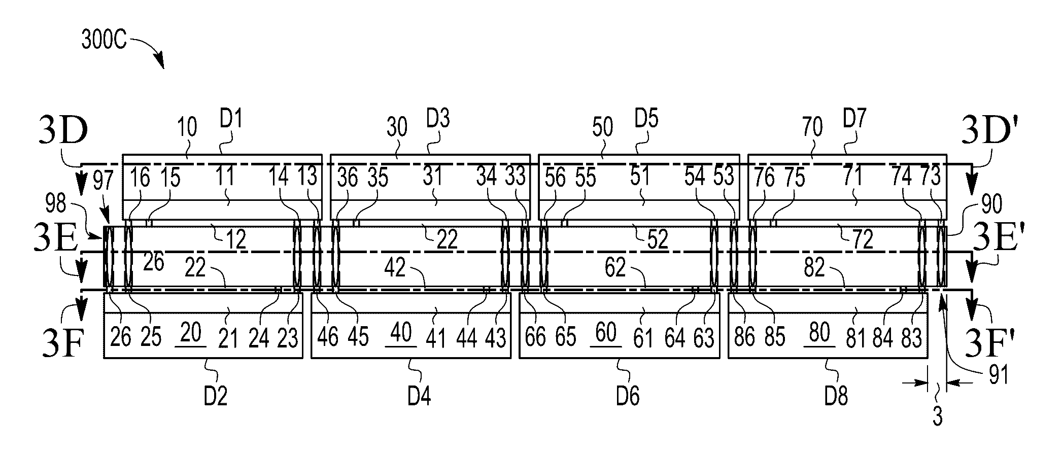
[0017]A method, apparatus, system and programming operation are disclosed for fabricating and / or operating a memory device, such as a thin low profile strip dual in-line memory module (DIMM). In selected embodiments, the strip DIMM includes a plurality of memory die formed in offset positions on opposite sides of a passive interposer structure. On each memory die, one or more conductive redistribution lines are formed at an interconnect surface to connect contact pads to one or more redistribution pads arrayed on opposite ends of the die. In addition, the memory die on the strip DIMM are connected together through a pattern of solder ball conductors formed in patterned openings through the passive interposer structure. By aligning the conductive redistribution lines, contact pads, and patterned openings in the passive interposer structure with the pattern of solder ball conductors, one or more bus signals may be routed to each memory die in the strip DIMM without requiring the forma...


PUM


Abstract

A low profile strip dual in-line memory module (200) includes a passive interposer support structure (90) with patterned openings (91-97) formed between opposing top and bottom surfaces, a plurality of memory chips (D1-D8) attached to the top and bottom surfaces, and vertical solder ball conductors (98) extending through the patterned openings to electrically connect the plurality of memory chips, where each memory chip has an attachment surface facing the passive interposer structure and a patterned array of horizontal conductors (e.g., 82-86) formed on the attachment surface with contact pads electrically connected to the plurality of vertical conductors to define at least one bus conductor that is electrically connected to each memory die in the first and second plurality of memory die.

Description

BACKGROUND OF THE INVENTION[0001]1. Field of the Invention[0002]The present invention is directed in general to field of integrated circuit memory devices. In one aspect, the present invention relates to a memory apparatus and method of operation.[0003]2. Description of the Related Art[0004]Computer systems increasingly use memory devices, such as dual-inline memory modules (DIMMs), to provide random access memory, not only for mounting RAM memory modules on a printed circuit board for plugging into computer motherboard, but also as a replacement for solid state drives (SSD) to store data on chips instead of on magnetic or optical discs. In a typical DIMM, a number of individual RAM chips—typically dynamic RAM (DRAM) chips—are mounted on a printed circuit board. However, there continue to be operational challenges and costs associated with reducing the size of such memory configurations while increasing the data storage density. As the complexity and density of DIMM integrated circu...

Claims


Application Information

Patent Timeline
Patent Type & Authority Patents(United States)
IPC IPC(8): H05K1/18H01L23/538H01L25/065H01L25/10H05K1/11G11C5/06H05K3/34
CPCH05K1/181H01L23/5384H01L25/0652H01L25/10H05K2201/097H05K2201/10159H05K2201/10378H05K2201/10545Y02P70/611G11C5/063H01L23/5385H01L2224/131H01L2224/13147H01L2224/16145H01L2224/16225H01L2225/06513H01L2225/06517H01L2225/06562H01L2924/1434H05K3/3415H01L2924/014H01L25/105H01L25/50H01L2224/16227H01L2224/16235H01L2225/06589H01L2225/1023H01L2225/107H01L2225/06572Y02P70/50H01L2924/00014
Inventor PELLEY, PERRY H.MCSHANE, MICHAEL B.PHAM, TIM V.
Owner NXP USA INC
Features
  • R&D
  • Intellectual Property
  • Life Sciences
  • Materials
  • Tech Scout
  • Unparalleled Data Quality
  • Higher Quality Content
  • 60% Fewer Hallucinations
Learn More