
Wafer treatment solution for edge-bead removal, edge film hump reduction and resist surface smooth, its apparatus and edge-bead removal method by using the same

a technology of edge film hump reduction and treatment solution, which is applied in the preparation of detergent mixture compositions, photomechanical equipment, instruments, etc., can solve the problems of incomplete etching or removal, image distortion, and large damage to semiconductor elements formed on the semiconductor wafer, so as to reduce the damage to a semiconductor element, improve the roughness of the film surface, and increase the efficiency of edge bead removal

Active Publication Date: 2016-11-29
KE I SHAN
View PDF20 Cites 4 Cited by
  • Summary
  • Abstract
  • Description
  • Claims
  • Application Information

AI Technical Summary

Benefits of technology

The present invention provides a solution for removing edge beads on semiconductor wafers during the manufacturing process. This solution helps to decrease damage to the semiconductor element and improve the smoothness of the film surface. The edge film hump thickness is reduced by at least 50%. This invention increases the efficiency of edge bead removal and solves the problems that were previously present in the art.

Problems solved by technology

The photoresist film humps may affect an exposure focus accuracy of a lithography process to cause image distortion.
Further, the photoresist film humps may also result in incompletely etching or removing after etching, and the residual humps may peel at following processes or cause that other films formed thereon are not easily attached, which is a contamination source of harmful particles at the following processes, and may cause a great damage on semiconductor elements formed on the semiconductor wafer.

Method used


Image

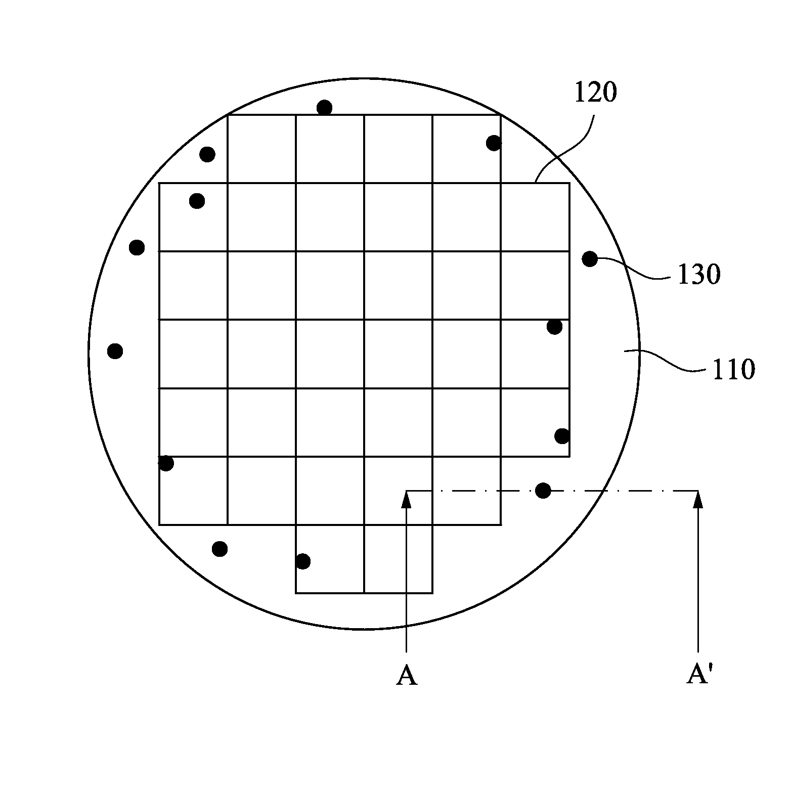
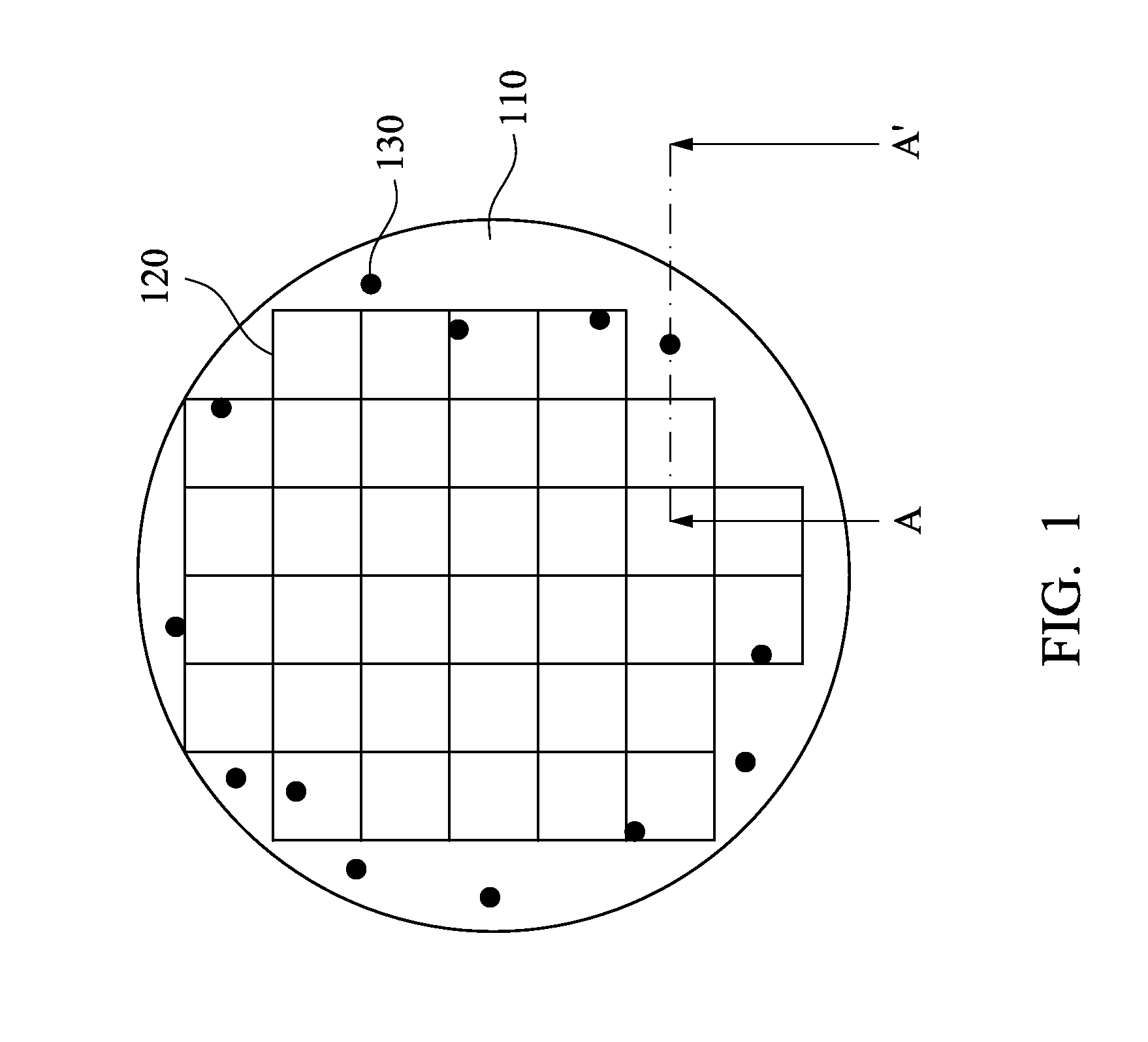
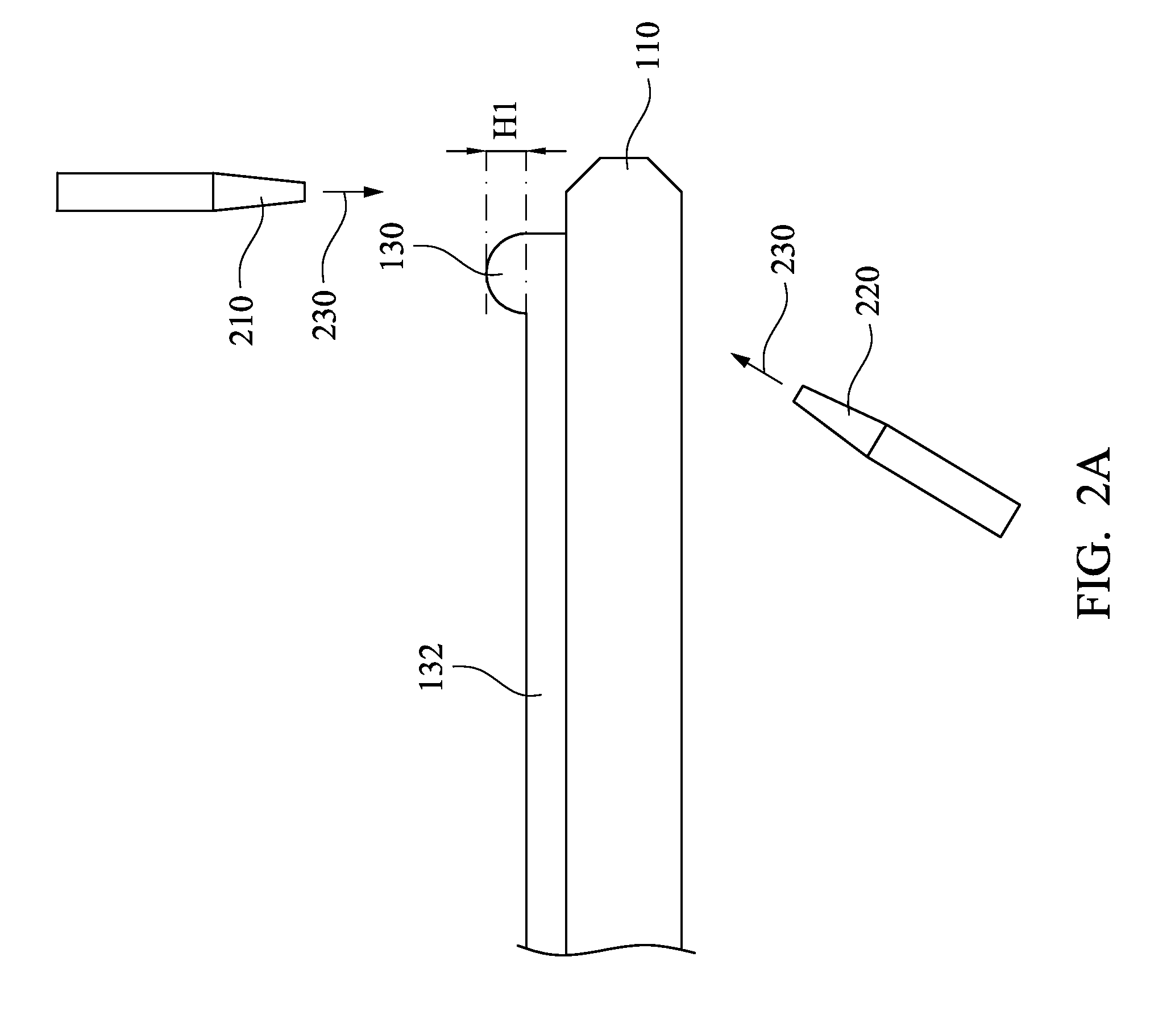
  • Wafer treatment solution for edge-bead removal, edge film hump reduction and resist surface smooth, its apparatus and edge-bead removal method by using the same
  • Wafer treatment solution for edge-bead removal, edge film hump reduction and resist surface smooth, its apparatus and edge-bead removal method by using the same
  • Wafer treatment solution for edge-bead removal, edge film hump reduction and resist surface smooth, its apparatus and edge-bead removal method by using the same

Examples


Embodiment Construction

[0048]The embodiments of the transparent heat-conducting structure and a method for manufacturing the same of the present disclosure are discussed in detail below, but not limited the scope of the present disclosure. The same symbols or numbers are used to the same or similar portion in the drawings or the description. And the applications of the present disclosure are not limited by the following embodiments and examples which the person in the art can apply in the related field.

[0049]The singular forms “a,”“an” and “the” used herein include plural referents unless the context clearly dictates otherwise. Therefore, reference to, for example, a metal layer includes embodiments having two or more such metal layers, unless the context clearly indicates otherwise. Reference throughout this specification to “one embodiment” means that a particular feature, structure, or characteristic described in connection with the embodiment is included in at least one embodiment of the present discl...


PUM

PropertyMeasurementUnit
temperatureaaaaaaaaaa
angleaaaaaaaaaa

Abstract

The present disclosure provides a wafer treatment solution for edge-bead removal, edge film hump reduction and resist surface smooth. The wafer treatment solution includes a solution and a fluorine-containing additive mixed in the solution. The fluorine-containing additive has a following formula (I): Rf—X—(CH2CH2O)m—R1 (I); or a following formula (II):An apparatus and a method by using the wafer treatment solution are also provided herein.

Description

RELATED APPLICATIONS[0001]This application claims priority to Taiwan Application Serial Number 103129216, filed Aug. 25, 2014, which is herein incorporated by reference.BACKGROUND[0002]Field of Invention[0003]The present disclosure relates to a wafer treatment solution for cleaning a semiconductor wafer. More particularly, the present disclosure relates to a fluorine-containing wafer treatment solution for cleaning a semiconductor wafer, and an apparatus and a method for surface roughness smoothing and removing and flattening at least one edge film hump at an edge of a semiconductor wafer by the wafer treatment solution.[0004]Description of Related Art[0005]In fabricating a general semiconductor element, a multi-layer structure is usually formed on a semiconductor wafer. In the process of forming the multi-layer structure, a photoresist layer is applied on the semiconductor wafer to perform a plurality of patterning processes of the semiconductor wafer. The photoresist layer is norm...

Claims


Application Information

Patent Timeline
Patent Type & Authority Patents(United States)
IPC IPC(8): C11D7/50H01L21/67C11D11/00H01L21/308H01L21/306
CPCH01L21/30604C11D7/5013C11D7/5018C11D11/0041H01L21/3081H01L21/6708G03F7/168C11D2111/20
Inventor LIN, YU-HSUN
Owner KE I SHAN
Learn More