Monolithically integrated self-aligned GaN-HEMTs and schottky diodes and method of fabricating the same

a technology of ganhemts and diodes, which is applied in the direction of diodes, semiconductor devices, electrical apparatus, etc., can solve the problems of increasing the cost of epitaxial wafers produced by this fabrication process, and achieve the effect of low resistan

Active Publication Date: 2016-12-06
HRL LAB
View PDF35 Cites 12 Cited by
  • Summary
  • Abstract
  • Description
  • Claims
  • Application Information

AI Technical Summary

Problems solved by technology

This two step process is complicated and thus increases cost of the epitaxial wafers being produced by this fabrication process.

Method used


Image

  • Monolithically integrated self-aligned GaN-HEMTs and schottky diodes and method of fabricating the same
  • Monolithically integrated self-aligned GaN-HEMTs and schottky diodes and method of fabricating the same
  • Monolithically integrated self-aligned GaN-HEMTs and schottky diodes and method of fabricating the same

Examples


Embodiment Construction

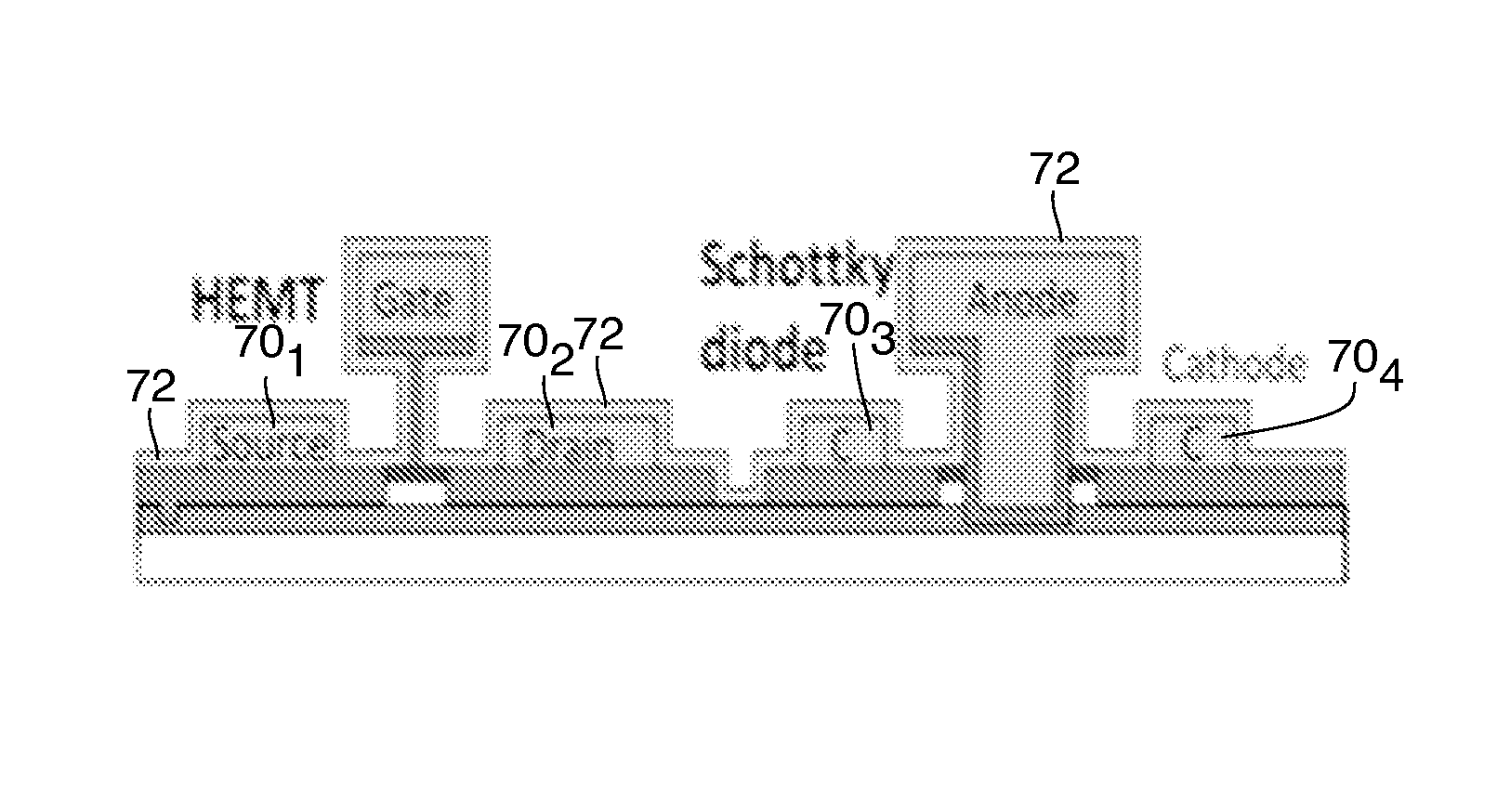
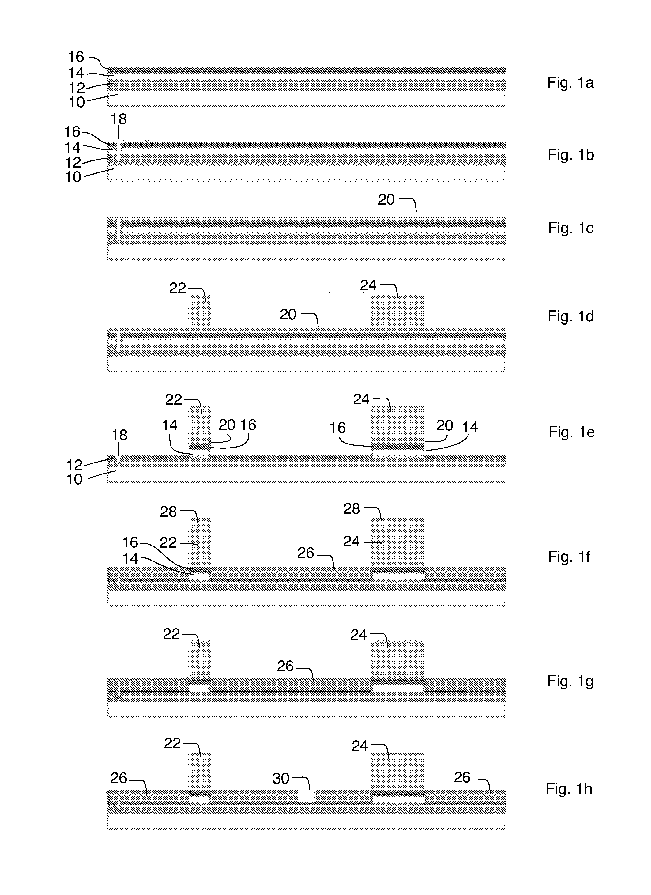
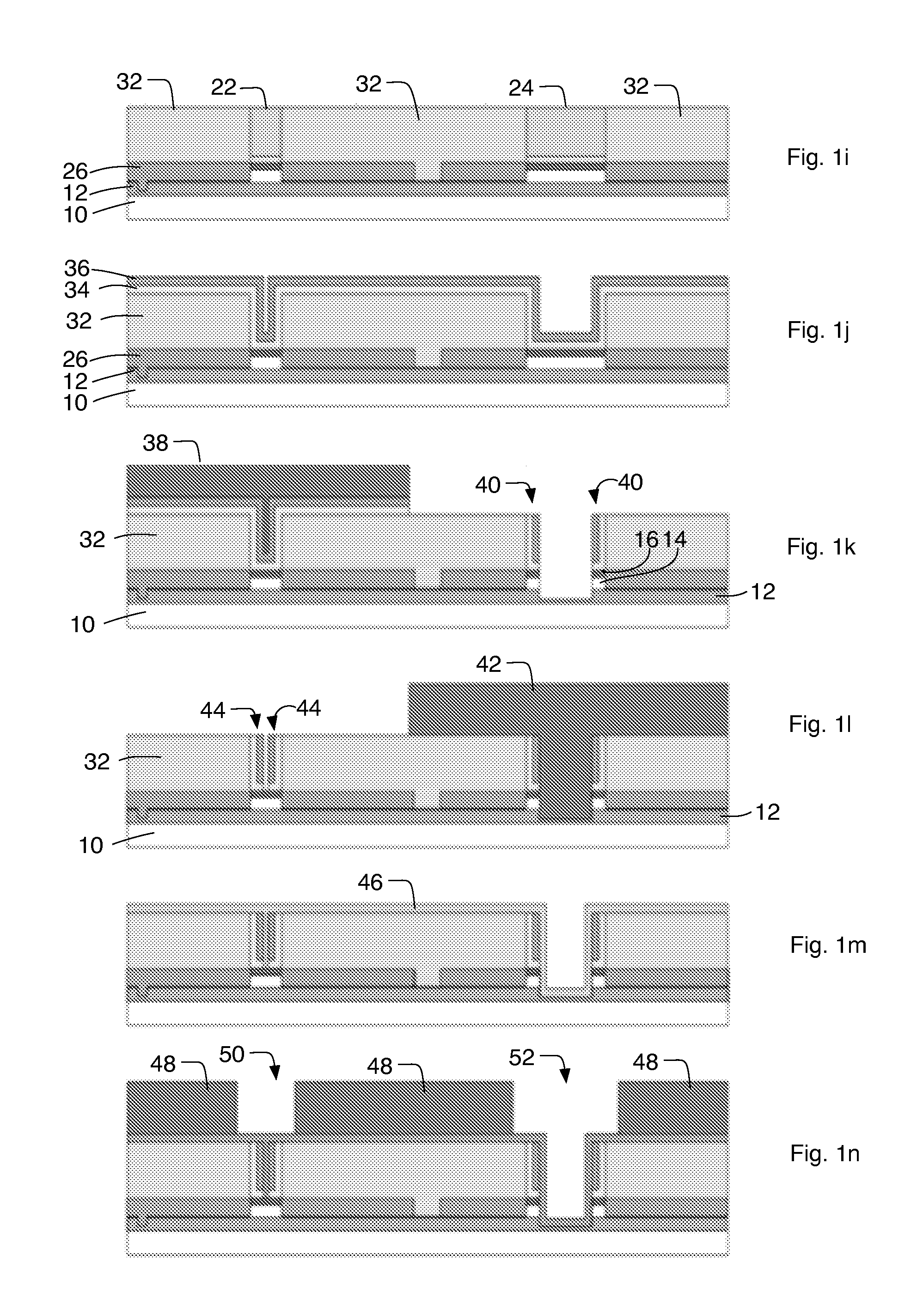
[0050]FIGS. 1a-1u show a fabrication processing flow sequence for making an embodiment of the integrated GaN HEMT / Schottky diode of the present invention. The first steps in the preferred fabrication sequence will now be described with reference to FIG. 1a. FIG. 1a shows GaN-based HEMT epitaxial growth by Molecular Beam Epitaxy (MBE) or Metal Organic Chemical Vapor Deposition (MOCVD) on a substrate 10 which may be sapphire, SiC, silicon, GaN, etc. The HEMT epitaxial layers preferably comprise an AlGaN back barrier layer 12 disposed on substrate 10, a GaN channel layer 14 disposed on layer 12, and an AlGaN top barrier layer 16 disposed on layer 14, all of which layers 12-16 are preferably grown by MBE or MOCVD. Alternatively, layer 12 can be GaN or InGaN / GaN, layer 14 can be InGaN or AlGaN, and layer 16 can be AlN or InAlN. The thickness of layer 16 is preferably about ⅕ of the gate length of the HEMT to suppress the short channel effect. The thickness of the layer 14 preferably rang...


PUM


Abstract

Monolithic integration of high-frequency GaN-HEMTs and GaN-Schottky diodes. The integrated HEMTs / Schottky diodes are realized using an epitaxial structure and a fabrication process which reduces fabrication cost. Since the disclosed process preferably uses self-aligned technology, both devices show extremely high-frequency performance by minimizing device parasitic resistances and capacitances. Furthermore, since the Schottky contact of diodes is formed by making a direct contact of an anode metal to the 2DEG channel the resulting structure minimizes an intrinsic junction capacitance due to the very thin contact area size. The low resistance of high-mobility 2DEG channel and a low contact resistance realized by a n+GaN ohmic regrowth layer reduce a series resistance of diodes as well as access resistance of the HEMT.

Description

STATEMENT REGARDING FEDERALLY SPONSORED RESEARCH OR DEVELOPMENT[0001]This invention was made pursuant to US Government Contact No. HR0011-09-C-0126 issued by DARPA and therefore the US Government may have certain rights in this invention.CROSS REFERENCE TO RELATED APPLICATIONS[0002]This application is a division of U.S. patent application Ser. No. 13 / 907,704 filed May 31, 2013 and originally entitled “Monolithically Integrated Self-Aligned GaN-HEMTs and Schottky Diodes and Method of Fabricating the Same”.[0003]This application is related to U.S. provisional patent application Ser. No. 61 / 772,753 filed Mar. 5, 2013 and entitled “Method Of Fabricating Self-Aligned Gate FETs” the disclosure of which is hereby incorporated herein by reference.[0004]This application is also related to U.S. patent application Ser. No. 12 / 792,529 filed Jun. 2, 2010 titled “Apparatus and Method for Reducing the Interface Resistance in GaN Heterojunction FETs” the disclosure of which is hereby incorporated h...

Claims


Application Information

Patent Timeline
Patent Type & Authority Patents(United States)
IPC IPC(8): H01L21/338H01L21/3205H01L29/423H01L21/02H01L29/205H01L29/47H01L29/201H01L29/20H01L29/66
CPCH01L29/66462H01L29/66143H01L29/2003H01L29/201H01L29/205H01L29/475H01L21/0254H01L21/02164H01L21/32051H01L29/42316H01L29/401H01L29/402H01L29/42376H01L29/66212H01L29/7786H01L21/8252H01L27/0629H01L27/0605H01L29/872
Inventor SHINOHARA, KEISUKEREGAN, DEAN C.
Owner HRL LAB
Why Eureka
Try Eureka