Electric circuit configuration having an MID circuit carrier and a connecting interface connected to it

a technology of connecting interface and circuit configuration, which is applied in the direction of printed element electric connection formation, coupling device connection, printed circuit non-printed electric components association, etc., can solve the problem of limited fashion of through-hole plating, and achieve high interconnection configuration density and high component density

Inactive Publication Date: 2017-01-31
ROBERT BOSCH GMBH
View PDF23 Cites 4 Cited by
  • Summary
  • Abstract
  • Description
  • Claims
  • Application Information

AI Technical Summary

Benefits of technology

[0005]Using the circuit configuration according to the present invention and the contact element group according to the present invention, it is possible to combine with one another injection-molded circuit carriers and printed circuit boards, using a simple technique and usual, known methods, without using costly external connecting elements. Owing to the combination, one may achieve that an electric circuit configuration unites the advantages of both the injection-molded circuit carriers, MID (molded interconnect devices) and the printed circuit boards, PCB (printed circuit board), so that three-dimensional circuit configurations, as are possible using MID, may be produced having a high interconnection configuration density and a high component density, as may be provided using PCB technique, using simple, already known production processes.
[0015]In order to provide a homogeneous electrical connection, both at least one printed circuit board section and a section of an electrical component, the connecting interface contact element and the surface of the MID circuit carrier are developed in complementary fashion to one another, in order further to provide the common arrangement of all contact elements of the electric circuit configuration. On printed circuit boards, since the connecting interface contact elements extend only slightly (less than 0.1 mm) away from the printed circuit board, the MID contact element may be developed in such a way that it extends away from the MID circuit carrier and along a direction leading to the printed circuit board or to the connecting interface. The MID contact elements formed in this way, which extend away from the MID circuit carrier, thus create sufficient distance between the MID circuit carrier and the printed circuit board to avoid or to reduce undesired contacting or capacitive coupling or inductive coupling.
[0018]Therefore, a material may be used as substrate for the MID circuit carrier which is not brittle at utilization temperatures and has at least partially elastic properties and suitable plastic properties, for three-dimensional shaping, the material being furthermore easily plastically deformable at higher temperatures or attaining flow properties.
[0020]The MID contact element may therefore be connected to an electrical component of the MID circuit carrier or to a line element of the MID circuit carrier. For the electrical conduction, the MID contact element may be connected by force locking, by form locking or by continuous material to one or to a plurality of line elements of the MID circuit carrier, or may be developed in one part with one or a plurality of line elements of the MID circuit carrier. The three-dimensional design possibilities of an MID circuit carrier, in particular, make possible the simple stamping of the MID contact elements, the MID contact elements being able to be developed in the same process in which the shape of the MID circuit carrier is formed.

Problems solved by technology

Printed circuit traces may provide a very dense connecting network, to be sure, but they are essentially limited to one plane, so that connections, which do not run in parallel to the printed circuit board, have to be provided using additional components or mechanical systems.
Based on the production method, MID substrates are only able to produce simple circuit structures having few components and a low area concentration.
Through-hole plating is possible only in limited fashion.

Method used


Image

  • Electric circuit configuration having an MID circuit carrier and a connecting interface connected to it
  • Electric circuit configuration having an MID circuit carrier and a connecting interface connected to it

Examples


Embodiment Construction

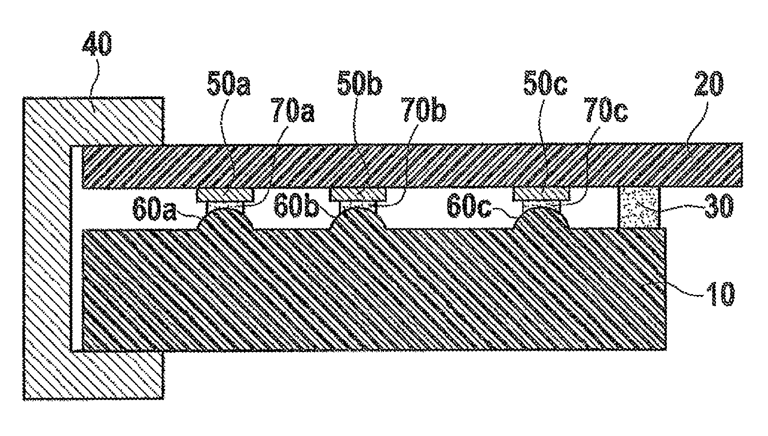
[0026]FIG. 1 shows an electric circuit configuration which includes a planar connecting interface 20 and an MID circuit carrier 10. Connecting interface 20 is connected to MID circuit carrier 10 via three individual contact pairs P, each contact pair producing a single electrical connection, which is separate from the electrical connections of the other electric contact pairs P. In FIG. 1, connecting interface 20 is developed by an insulating carrier or by a substrate and a copper outer layer situated on it, which form a printed circuit board. The copper outer layer forms contact areas or pads, which may be developed in one part with printed circuit boards (not shown).

[0027]Each electric contact pair includes a connecting interface contact element, an electrical contact element which includes conductive material, for example, conductive adhesive material, as well as MID contact elements 60a-c. The electrical connecting element, which in FIG. 1 is made of a conductive adhesive materi...


PUM


Abstract

An electric circuit configuration having an MID circuit carrier and a connecting interface, the connecting interface being situated on a surface of the MID circuit carrier. The electric circuit configuration further includes at least one electrical contact pair having at least one connecting interface contact element and at least one MID contact element that is provided on the surface and is situated on the connecting interface contact element. The exemplary embodiments and / or exemplary methods of the present invention further relates to a contact element group having at least one electrical contact element for the electrical contacting of an MID circuit carrier, which is developed on a surface of an MID circuit carrier, is electrically connected to it, and extends away from the surface. The at least one contact element is connected to a line element of the MID circuit carrier.

Description

FIELD OF THE INVENTION[0001]The present invention relates to electric connections using printed circuit boards and electric connections using injection-molded circuit carriers, MID's.BACKGROUND INFORMATION[0002]The use of printed circuit boards, PCB's, is a standard method for connecting electrical components. The connections are specified by printed circuit traces which run on a surface of a planar printed circuit board. Printed circuit boards offer good protection from electrostatic discharges and have good properties with respect to electromagnetic compatibility. Printed circuit traces may provide a very dense connecting network, to be sure, but they are essentially limited to one plane, so that connections, which do not run in parallel to the printed circuit board, have to be provided using additional components or mechanical systems.[0003]Three-dimensional printed circuit board structures may be produced using injection-molded circuit carriers, MID's, whereby a housing and a ci...

Claims


Application Information

Patent Timeline
Patent Type & Authority Patents(United States)
IPC IPC(8): H05K1/11H05K3/36H05K1/18H01R12/71H01R13/405H05K1/02H05K3/32H05K3/40H01R12/50
CPCH05K3/368H01R12/714H05K1/119H05K1/181H01R13/405H05K1/0284H05K3/321H05K3/4007H05K2201/09045H05K2201/09118H05K2201/10393
Inventor KOPF, STEFANROHDE, HARTMUT
Owner ROBERT BOSCH GMBH
Why Eureka
Try Eureka