Composite protective layer for photoelectrode structure, photoelectrode structure including the composite protective layer, and photoelectrochemical cell including photoelectrode structure

a technology of photoelectrode structure and composite protective layer, which is applied in the direction of electrochemical cell, energy input, electrochemical coating, etc., can solve the problem of limit in using semiconductor materials capable of exerting better photoelectric efficiency, and achieve the effect of improving the lifespan of the photoelectrode structur

Inactive Publication Date: 2017-02-14
SAMSUNG ELECTRONICS CO LTD
View PDF15 Cites 2 Cited by
  • Summary
  • Abstract
  • Description
  • Claims
  • Application Information

AI Technical Summary

Benefits of technology

[0008]Provided is a composite protective layer for a photoelectrode structure for improving a lifespan of a photoelectrode structure for decomposing water.

Problems solved by technology

Also, because only materials stable in the aqueous electrolyte may be used as the materials for the photoelectrode, there is a limitation in using semiconductor materials capable of exerting better photoelectric efficiency.

Method used


Image

  • Composite protective layer for photoelectrode structure, photoelectrode structure including the composite protective layer, and photoelectrochemical cell including photoelectrode structure
  • Composite protective layer for photoelectrode structure, photoelectrode structure including the composite protective layer, and photoelectrochemical cell including photoelectrode structure
  • Composite protective layer for photoelectrode structure, photoelectrode structure including the composite protective layer, and photoelectrochemical cell including photoelectrode structure

Examples


example 1

Manufacturing a Photoelectrode Structure

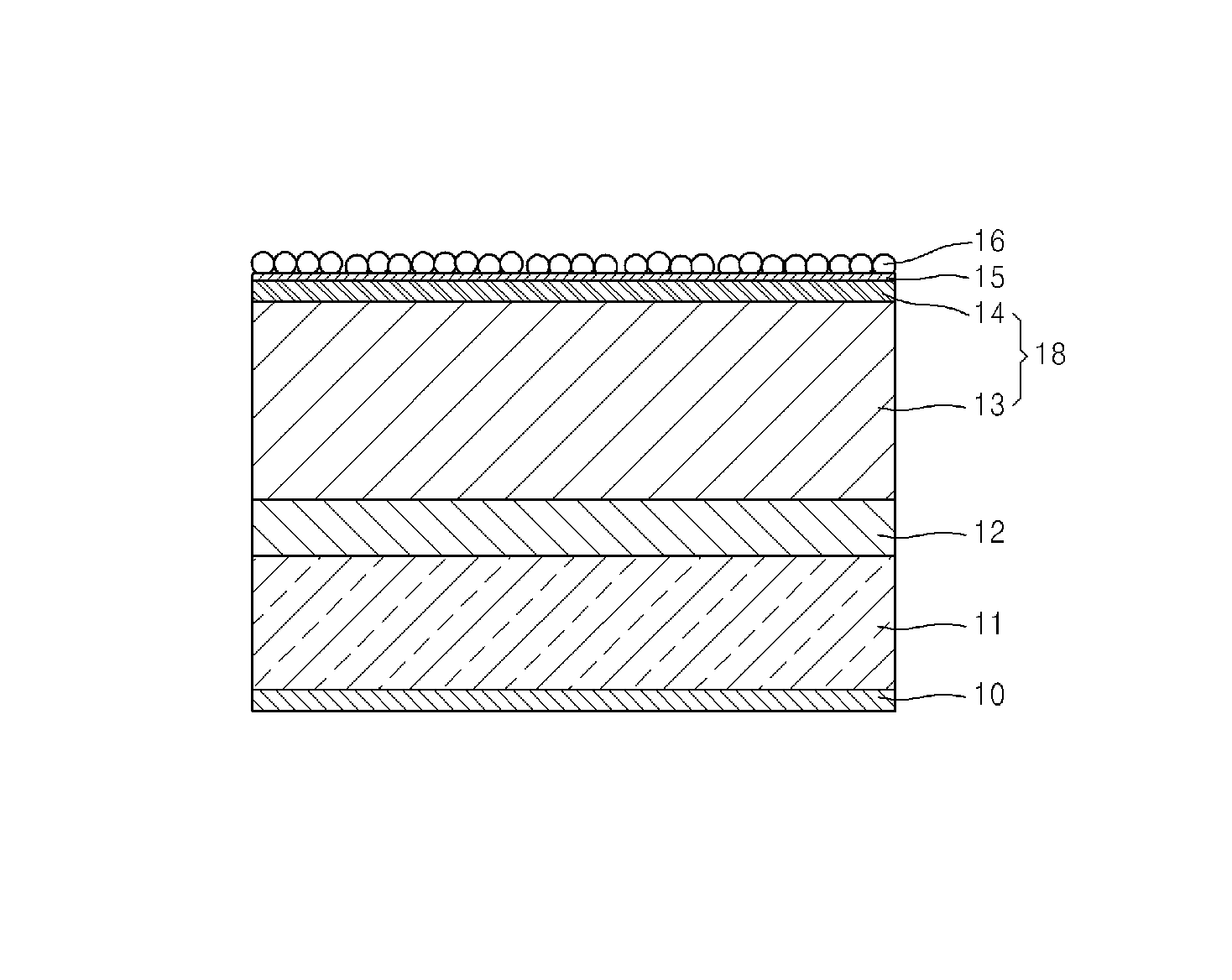
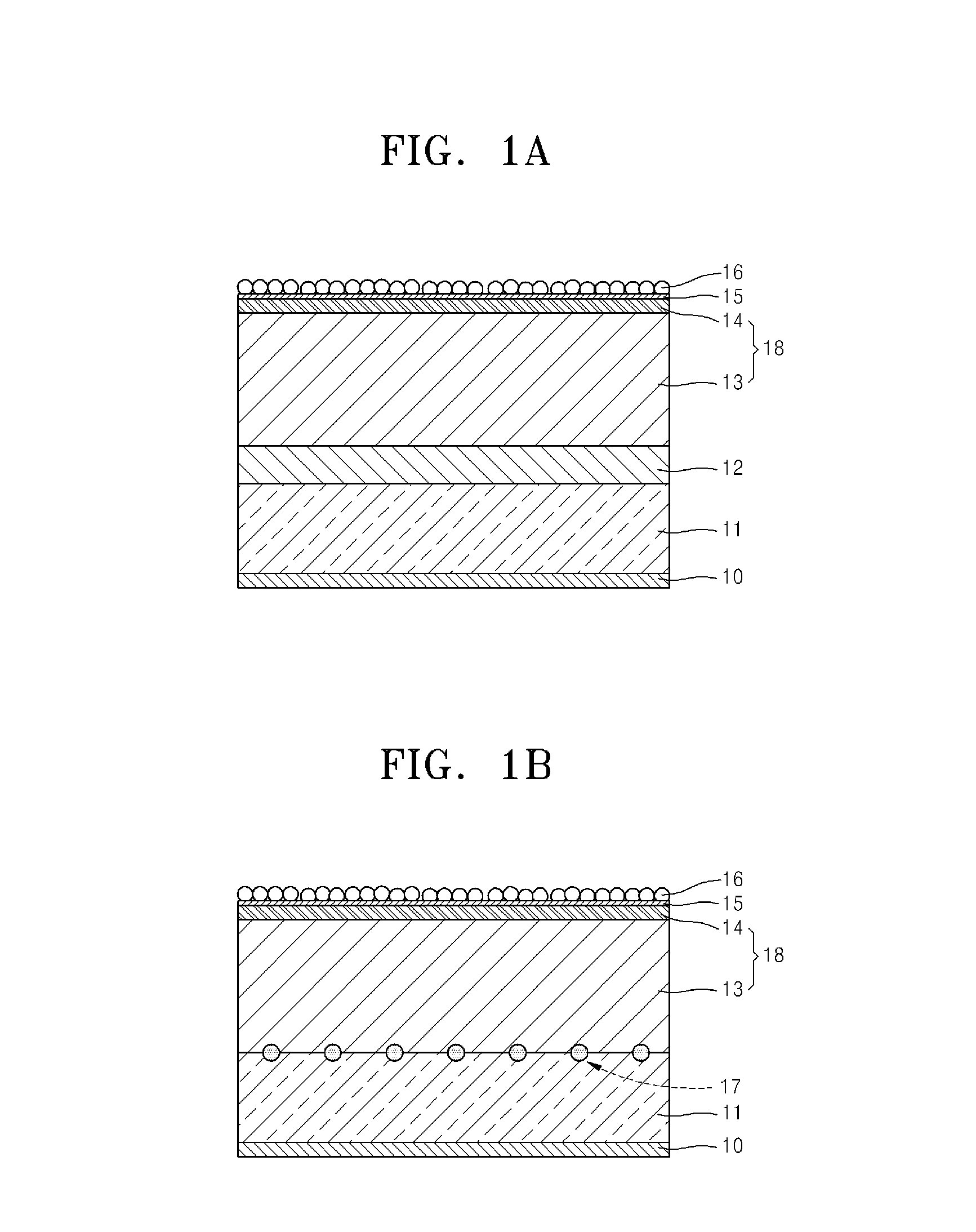
[0136]An FTO film formed on a glass substrate was used as an electrode. On the FTO film, Cu2O was deposited to form a light absorbing layer having a thickness of about 5 μm. After the light absorbing layer was treated with hydrogen peroxide to remove organic material on a surface of the light absorbing layer, the light absorbing layer was heat treated at a temperature of about 450° C. for about 30 minutes under a vacuum condition.

[0137]On the light absorbing layer, a hole blocking layer having a thickness of about 70 nm was formed by sputtering TiO2 and thus an FTO film (hereinafter, an FTO glass film) / a Cu2O film / a TiO2 structure formed on the glass substrate was manufactured.

[0138]Separately, on a Cu foil physical protective layer having a thickness of about 20 μm, Ta was deposited to form a Ta chemical protective layer having a thickness of about 100 nm, to thereby form a composite protective layer (Ta thin film chemical protective layer / Cu...

example 2

Manufacturing a Photoelectrode Structure (a Photoanode)

[0141]A composite protective layer was formed by laminating a Ta film where Ta is deposited in a thickness of 100 nm and a Cu foil having a thickness of 20 μm. A Cu foil of the composite protective layer was bonded to an In foil using a roll press, and a structure of In layer / Cu foil / Ta thin film / Ta native oxide film was obtained.

[0142]The In layer of the In layer / Cu foil / Ta thin film / Ta structure was bonded to a p-type silicon layer of the light absorbing layer wherein an n-type silicon layer and the p-type silicon layer are sequentially laminated, and pressurized at a temperature of about 200° C. to form a structure including an n-type silicon layer / p-type silicon layer / In layer / Cu foil / Ta thin film / Ta native oxide film.

[0143]On a Ta native oxide film of the n-type silicon layer / p-type silicon layer / In layer / Cu foil / Ta thin film / Ta native oxide film structure, a Co3O4 catalyst was deposited to form a Co3O4 layer to form an n-t...


PUM

PropertyMeasurementUnit
electrical conductivityaaaaaaaaaa
thicknessaaaaaaaaaa
thicknessaaaaaaaaaa

Abstract

A composite protective layer for a photoelectrode, the composite protective layer including a chemical protective layer; and a physical protective layer, wherein the chemical protective layer has corrosion rate of 0.1 Coulombs per square centimeter per 10 hours or less when evaluated at a water decomposition potential, and the physical protective layer has a moisture transmittance rate of 0.001 grams per square meter per day or less and has an electrical conductivity.

Description

CROSS-REFERENCE TO RELATED APPLICATION[0001]This application claims priority to and the benefit of Korean Patent Application No. 10-2013-0010097, filed on Jan. 29, 2013, and all the benefits accruing therefrom under 35 U.S.C. §119, the content of which is incorporated herein in its entirety by reference.BACKGROUND[0002]1. Field[0003]The present disclosure relates to composite protective layer for a photoelectrode structure, a photoelectrode structure including the composite protective layer, and a photoelectrochemical cell (“PEC”) including the photoelectrode structure.[0004]2. Description of the Related Art[0005]A photoelectrochemical cell (“PEC”) that obtains hydrogen and oxygen through decomposition of water by using solar energy is environmentally friendly because sunlight and water are used as an energy source and a reactant, respectively.[0006]In most conventional PECs, a photoelectrode directly contacts an aqueous electrolyte and as a result, performance of the PECs is reduce...

Claims


Application Information

Patent Timeline
Patent Type & Authority Patents(United States)
IPC IPC(8): C25B11/04C01B3/04C25B1/00
CPCC25B11/0478C01B3/042C25B1/00C25B1/003Y02E60/364Y02E60/368Y02P20/135Y10T428/12611Y10T428/12819C25B1/55C25B11/091Y02E60/36Y02P20/133H01M14/00
Inventor KIM, TAE-GONLEE, JEONG-HEEIM, SEOUNG-JAEKIM, TAE-HYUNG
Owner SAMSUNG ELECTRONICS CO LTD
Why Eureka
Try Eureka