Spin wave device and logic circuit using spin wave device
a logic circuit and spin wave technology, applied in the direction of power consumption reduction, pulse technique, instruments, etc., can solve the problems of processing limits and power consumption reduction, and achieve the effects of low power consumption, high speed, and miniaturization
- Summary
- Abstract
- Description
- Claims
- Application Information
AI Technical Summary
Benefits of technology
Problems solved by technology
Method used
Image
Examples
first embodiment
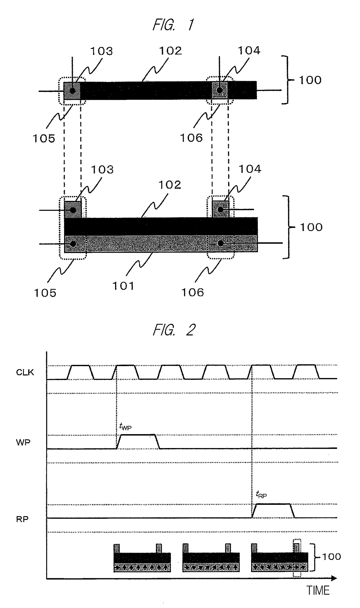
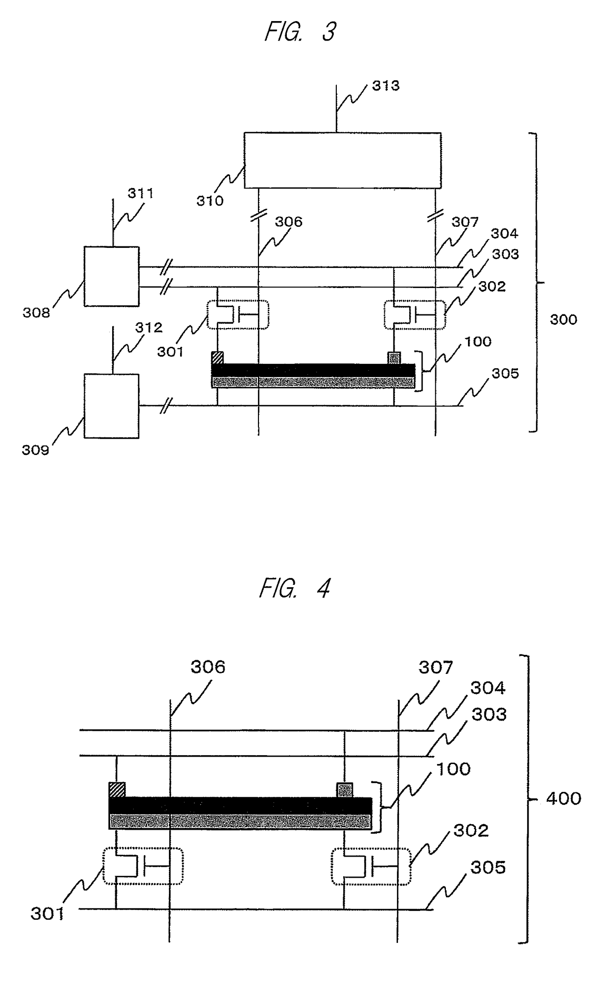
[0034]A spin wave device is a device that converts an input signal (“0” or “1”) into a spin wave corresponding to “0” or “1”, propagates the spin wave to an output unit present in a place apart from an input unit, and read out. Major characteristics are that consumption of electric power is extremely small in a portion that generates the spin wave corresponding to the input signal, a portion that propagates the spin wave, and a portion that outputs the spin wave. It is possible to convert two input signals respectively into spin waves, cause the two spin waves to interfere with each other to cause the spin waves to operate like a logic gate, and output logic. By disposing the logic gate by the spin wave device in multiple stages, it is possible to form a logic circuit. In the following explanation, an operation principle of the spin wave device is explained with reference to the figures.
[0035]According to a viewpoint of the invention, as shown in FIG. 1, a spin wave device 100 inclu...
second embodiment
[0056]In the spin wave device 100 described in the first embodiment, the spin wave having the information of “1” is the wave approximately π / 2 different in the phase from the spin wave having the information of “0”. According to another viewpoint of the invention, the spin wave having the information of “1” may be a wave phase-shifted by π from the spin wave having the information “0”. A basic structure of the spin wave device 100 described in a second embodiment is the same as the basic structure shown in FIG. 1. Operation timings of a clock signal, a WP applied from the first electrode 103, and an RP applied from the second electrode 104 are basically the same as the operation timings in FIG. 5. FIG. 8 is a diagram showing a temporal change of an output signal obtained by measuring, via a reference resistor, as a voltage, the magnitude of an output current at the time when a micro-voltage is applied in the film surface perpendicular direction of the output portion 106. In an outpu...
third embodiment
[0057]In the spin wave device 100 described in the first embodiment and the second embodiment, the information of “0” or “1” of the spin wave is characterized by the phase of the spin wave. According to another viewpoint of the invention, information of “0” or “1” of the spin wave can be characterized by the amplitude of the spin wave. FIG. 9 is schematically shows a spin wave having information of “0” and “1” propagated to the output portion 106 and a magnetization direction of the first ferromagnetic layer 101 at that point. In an example shown in FIG. 9, the amplitude of the spin wave having the information of “0” is plus. At t1, a magnetization direction of a portion of the first ferromagnetic layer 101 included in the output portion 106 is a parallel rightward direction with respect to a film surface. On the other hand, the amplitude of the spin wave having the information of “1” is minus. At t1, the magnetization direction of a portion of the first ferromagnetic layer 101 incl...
PUM
 Abstract
Description
Claims
Application Information


