
Power semiconductor module and method for cooling power semiconductor module

a technology of power semiconductor modules and power semiconductors, applied in the direction of dielectric characteristics, printed circuit aspects, association of printed circuit non-printed electric components, etc., can solve the problem of reducing the thermal resistance rsub>, achieve effective flow control of coolant, improve convective heat transfer, and improve the effect of porosity

Active Publication Date: 2017-03-28
ABB (SCHWEIZ) AG
View PDF7 Cites 0 Cited by
  • Summary
  • Abstract
  • Description
  • Claims
  • Application Information

AI Technical Summary

Benefits of technology

The patent text describes a cooling system for electronic packages using a layer of thermally conductive foam (TCF). By adjusting the TCF's porosity, a specific flow path can be assigned to each package component, resulting in more uniform heat distribution and reduced thermal-related failures. The design also minimizes pressure drop and is easy to manufacture and install. This cooling system is lightweight, cost-effective, and has good mechanical and structural properties.

Problems solved by technology

Such an implementation may also reduce the thermal resistance Rth of the package [3].

Method used


Image

  • Power semiconductor module and method for cooling power semiconductor module
  • Power semiconductor module and method for cooling power semiconductor module
  • Power semiconductor module and method for cooling power semiconductor module

Examples


Embodiment Construction

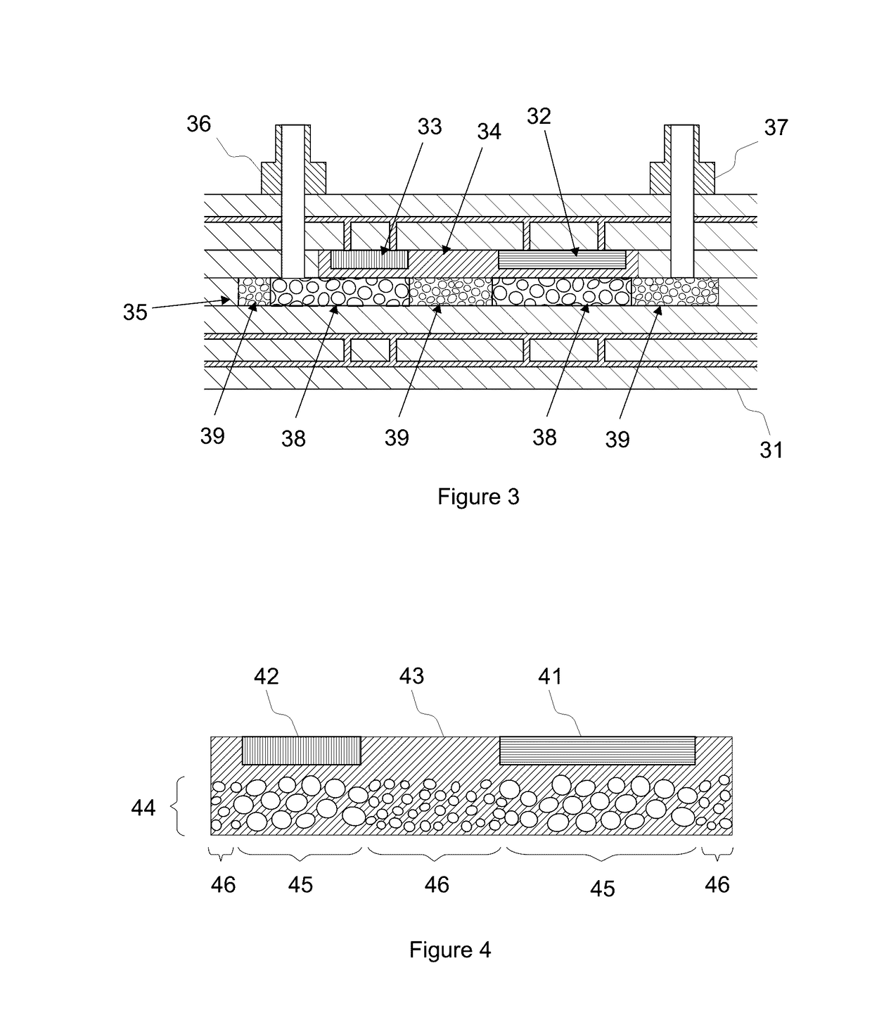
[0016]The present disclosure presents a power semiconductor module comprising a printed circuit board (PCB). The PCB comprises at least one power semiconductor device and thermally conducting foam (TCF) embedded in the printed circuit board. The power semiconductor device may be a diode or a semiconductor switch, for example. The thermally conducting foam refers to a porous material that is thermally conducting and through which coolant can pass. The thermally conducting foam may be open-cell metal foam made of aluminium or copper, for example.

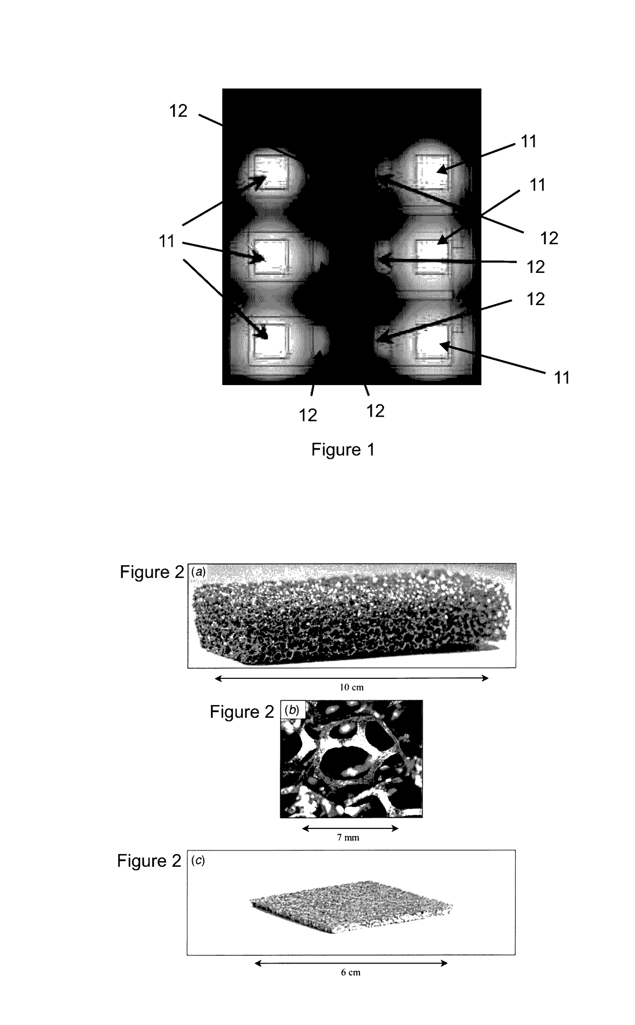
[0017]FIGS. 2(a) to 2(c) show details of an exemplary block of aluminium foam. FIG. 2(a) shows an aluminium foam block, which measures 10.0 cm×4.0 cm×1.5 cm, and is 92% porous (10 pores per linear inch=6.9 mm pore diameter). FIG. 2(b) shows a magnified view of a single pore of the foam block of FIG. 2(a). The pore size (i.e., the approximate diameter of the pore) is 7 mm in FIG. 2b. FIG. 2(c) shows the exemplary aluminium foam block as depicte...


PUM

PropertyMeasurementUnit
power ratingsaaaaaaaaaa
pore diameteraaaaaaaaaa
diameteraaaaaaaaaa

Abstract

The present disclosure relates to a power semiconductor module comprising a printed circuit board (PCB), and to method of cooling such a power semiconductor module. The module comprises a power semiconductor device and an island of thermally conducting foam embedded into the printed circuit board. The power semiconductor device and the island of thermally conducting foam are positioned on top of each other, and the island is arranged to form a path for a flowing coolant cooling the power semiconductor device.

Description

FIELD OF THE INVENTION[0001]The present invention relates to power semiconductor modules and particularly to cooling of power semiconductor modules.BACKGROUND INFORMATION[0002]Power electronic devices in a lower power range (e.g. devices with power ratings less than about 50 kW) are often based on printed circuit board (PCB) constructions. Traces of both a main power circuit and signal electronics may be integrated into the PCB. Electrical components, such as semiconductor switches, passive components, and integrated circuits (IC), are typically attached to the surface of the PCB by soldering. By using PCBs, mass production costs may be reduced, while device compactness may be increased.[0003]As more components are integrated to PCBs, power dissipation per area unit of the PCBs also increases. Further, components on a PCB may have diverse cooling demands, particularly if the PCB comprises embedded power semiconductors. As a result, localized hot spots may appear on the PCB. FIG. 1 s...

Claims


Application Information

Patent Timeline
Patent Type & Authority Patents(United States)
IPC IPC(8): H01L23/34H05K1/02H01L23/31H01L23/473H01L23/538H05K1/18H05K3/46
CPCH01L23/473H01L23/3121H01L23/5389H05K1/0272H01L2924/0002H05K1/185H05K3/4697H05K2201/0116H05K2201/064H01L2924/00H01L2224/24137H01L2224/32245H01L2224/73267H01L2224/92244H01L2924/15153
Inventor KEARNEY, DANIELAGOSTINI, FRANCESCOCOTTET, DIDIERTORRESIN, DANIELEHABERT, MATHIEU
Owner ABB (SCHWEIZ) AG
Learn More