Photonic transceiving device package structure

Active Publication Date: 2017-06-06
MARVELL ASIA PTE LTD
View PDF6 Cites 21 Cited by
  • Summary
  • Abstract
  • Description
  • Claims
  • Application Information

AI Technical Summary

Benefits of technology

The present patent describes a small package structure for a photonic transceiver that has several advantages. Firstly, it includes a modified holder for supporting LC receptacles and a clip for maintaining the LC ferrule to stub contact in TOSAs. A dust cap is added to protect wire bonding between the chip and the PCB, and it also acts as part of a fiber-routing structure to change fiber routing from short direct coupling to long routed coupling with the chip to increase reliability. Other changes are made to improve the assembly, such as modifying the mechanical design and integrating electronics chips. Overall, this package structure makes it easier to assemble and use photonic transceivers.

Problems solved by technology

But Internet and mobile applications continuously demand a huge amount of bandwidth for transferring photo, video, music, and other multimedia files.
Serial link performance is limited by the channel electrical bandwidth and the electronic components.
Stacking chips into so-called 3-D ICs promises a one-time boost in their capabilities, but it's very expensive.

Method used


Image

  • Photonic transceiving device package structure
  • Photonic transceiving device package structure
  • Photonic transceiving device package structure

Examples


Embodiment Construction

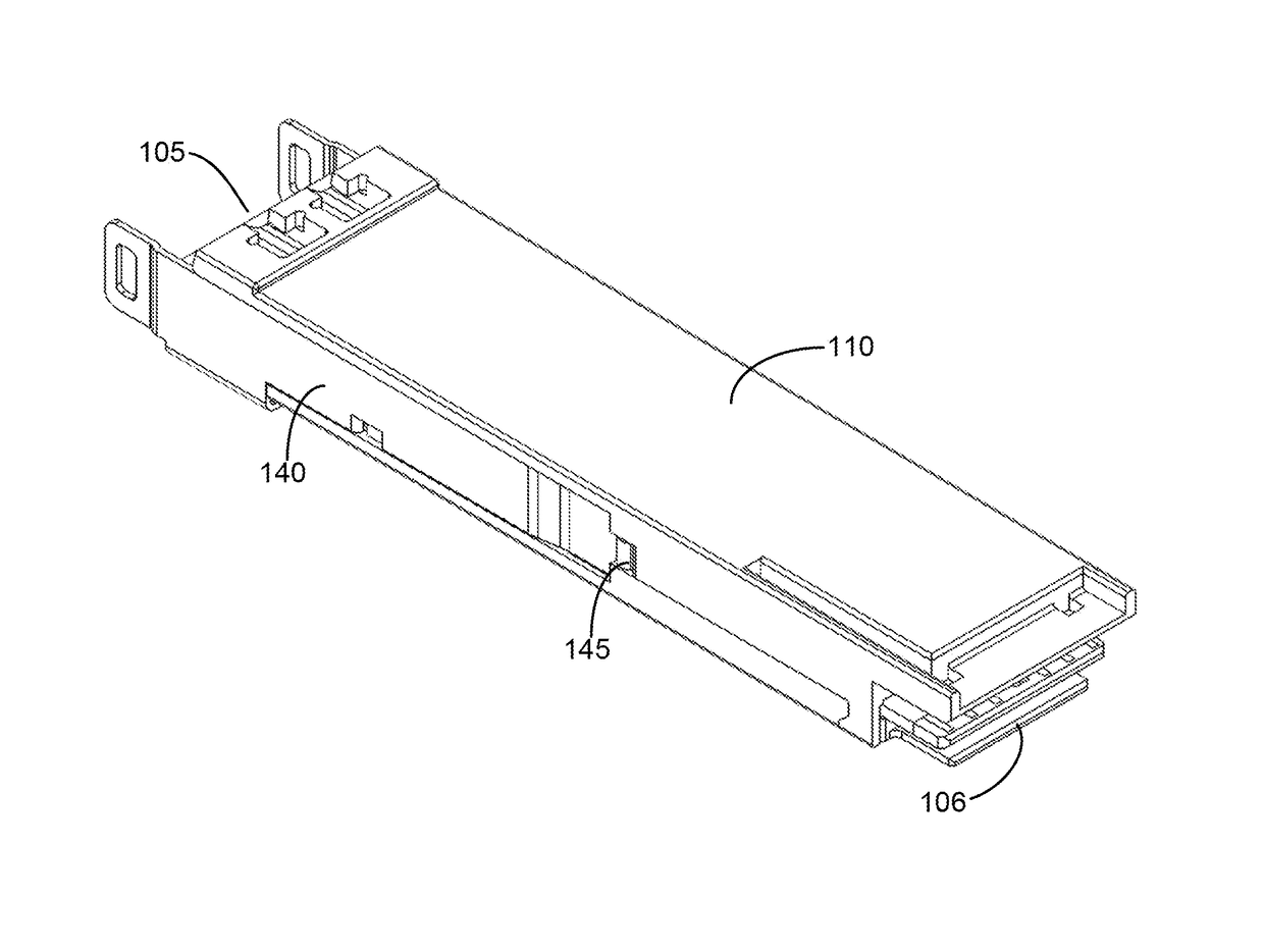
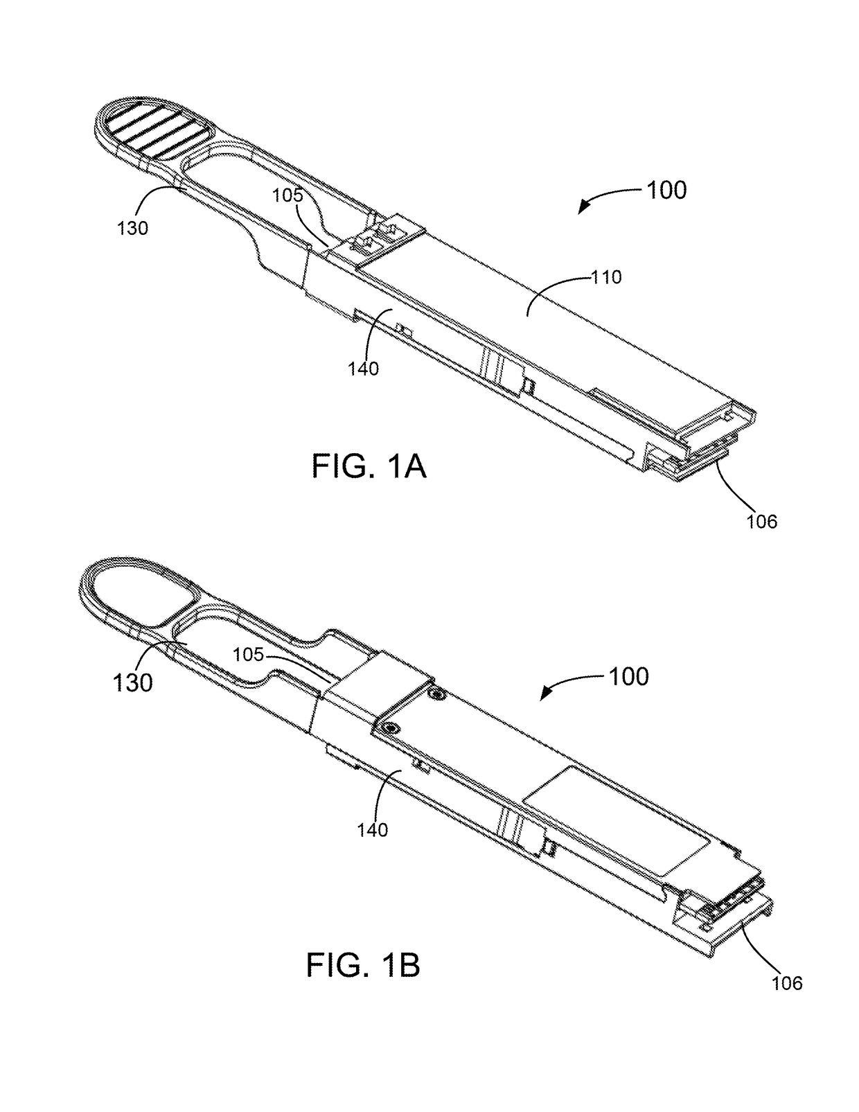
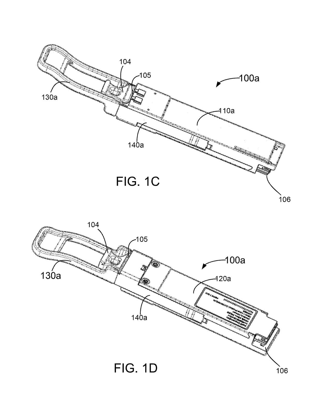
[0040]The present disclosure is related to a photonic transceiver package structure, more particularly, to a silicon photonic transceiver package structure in Quad Small Form-factor Pluggable (QSFP) specification adapted with multiple thermoelectric-cooled transmitter optical sub-assembly (TEC-TOSA) laser devices disposed upside down to keep heat sinks away from a printed circuit board (PCB) and laid reversely in orientation of laser output port relative to optical input / output port of the transceiver. In certain embodiments, the invention is applied for high bandwidth optical communication, though other applications are possible.

[0041]The following description is presented to enable one of ordinary skill in the art to make and use the invention and to incorporate it in the context of particular applications. Various modifications, as well as a variety of uses in different applications will be readily apparent to those skilled in the art, and the general principles defined herein ma...


PUM


Abstract

An apparatus for packaging a photonic transceiver. The apparatus includes a case having a base member, two partial side members, and a lid member to provide a spatial volume with an opening at a back end of the base member. Additionally, the apparatus includes a PCB installed inside the spatial volume over the base member with a pluggable connector at the back end. The apparatus includes one or more optical transmitting devices being mounted upside-down via a flex circuit board bended 180 degrees inward to a backside of the PCB and including a built-in TEC module in contact with the lid member. Furthermore, the apparatus includes a silicon photonics chip including a fiber-to-silicon attachment module, mounted on the PCB and coupled to a modulation driver module and a trans-impedance-amplifier module. Moreover, the apparatus includes an optical input port and output port being back connected to the fiber-to-silicon attachment module.

Description

CROSS-REFERENCE TO RELATED APPLICATIONS[0001]The present application is a continuation-in part application of and incorporates by reference, for all purposes, the following patent application: U.S. patent application Ser. No. 14 / 789,290, filed Jul. 1, 2015, now issued as U.S. Pat. No. 9,496,969 on Nov. 15, 2016.BACKGROUND OF THE INVENTION[0002]The present disclosure is related to a photonic transceiver package structure, more particularly, to a silicon photonic transceiver package structure that conforms to the QSFP specification with modified TOSA laser assembly.[0003]As science and technology are progressing rapidly, processing speed and capacity of the computer increase correspondingly. The communication transmission or reception using the traditional cable is limited to bandwidth and transmission speed of the traditional cable, but the mass information transmission required in modern life causes the traditional communication transmission overload. To address such requirements, t...

Claims


Application Information

Patent Timeline
IPC IPC(8): H04B10/00G02B6/32G02B6/38H04B10/40G02B6/42H05K3/30H04B1/3827H04B10/50
CPCG02B6/4257H04B10/40H04B10/503G02B6/4292G02B6/4284G02B6/428G02B6/4295G02B6/3849G02B6/32G02B6/4206G02B6/4208G02B6/3893H05K3/30H04B1/3833G02B6/4251G02B6/4286G02B6/4271G02B6/421G02B6/4246G02F1/2255G02B6/4281
Inventor NAGARAJAN, RADHAKRISHNAN L.LI, PENG-CHIHKATO, MASAKITOGAMI, CHRIS
Owner MARVELL ASIA PTE LTD
Why Eureka
Try Eureka