Semiconductor phosphor nanoparticle, semiconductor phosphor nanoparticle-containing glass, light emitting device, and light emitting element

a technology of semiconductor phosphor and phosphor nanoparticles, which is applied in the direction of crystal growth process, polycrystalline material growth, light emitting compositions, etc., can solve the problems of nanoparticle surface, quantum efficiency degradation, and quantum efficiency degradation, and achieve the effect of quantum efficiency reduction

Inactive Publication Date: 2017-07-25
SHARP KK
View PDF16 Cites 0 Cited by
  • Summary
  • Abstract
  • Description
  • Claims
  • Application Information

AI Technical Summary

Benefits of technology

[0013]However, when the semiconductor phosphor nanoparticle of Japanese National Patent Publication No. 2010-535262 is glass-sealed using organoalkoxysilane or resin-sealed using a macromolecular material, it is decreased in quantum efficiency.
[0015]Furthermore, in various processes using the phosphor nanoparticle, if water can be used as a solvent, there are merits such as low environmental burden and low cost. Accordingly, there is a demand for a phosphor nanoparticle having good dispersibility in an aqueous solution. However, the phosphor nanoparticle of Japanese National Patent Publication No. 2010-535262 does not have satisfactory dispersibility in water.
[0016]Accordingly, a first object of the present invention is to provide a phosphor nanoparticle and light emitting element that have satisfactory quantum efficiency even when glass-sealed or resin-sealed, and furthermore, have excellent dispersibility in water.
[0018]A second object of the present invention is to provide a semiconductor phosphor nanoparticle, a semiconductor phosphor nanoparticle-containing glass, and a light emitting device using that semiconductor phosphor nanoparticle, that exhibit high emission efficiency and also have excellent chemical stability.

Problems solved by technology

However, when the semiconductor phosphor nanoparticle of Japanese National Patent Publication No. 2010-535262 is glass-sealed using organoalkoxysilane or resin-sealed using a macromolecular material, it is decreased in quantum efficiency.
This is believed to cause defects in the nanoparticle's surface and result in impaired quantum efficiency.
However, the phosphor nanoparticle of Japanese National Patent Publication No. 2010-535262 does not have satisfactory dispersibility in water.

Method used


Image

  • Semiconductor phosphor nanoparticle, semiconductor phosphor nanoparticle-containing glass, light emitting device, and light emitting element
  • Semiconductor phosphor nanoparticle, semiconductor phosphor nanoparticle-containing glass, light emitting device, and light emitting element
  • Semiconductor phosphor nanoparticle, semiconductor phosphor nanoparticle-containing glass, light emitting device, and light emitting element

Examples


first embodiment

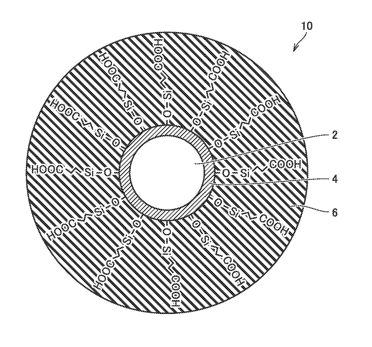
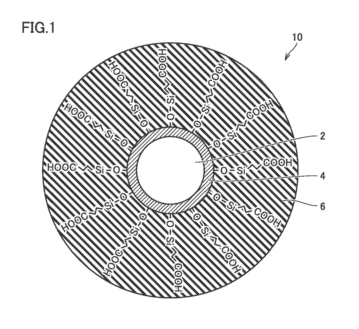
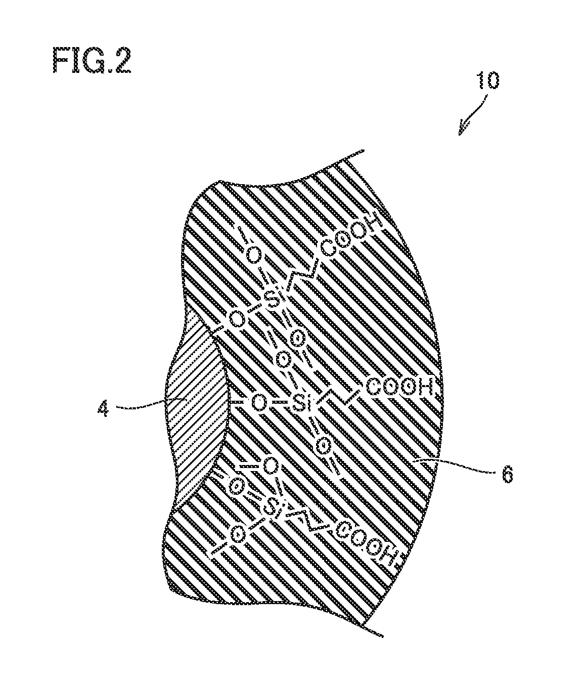
[0037]A semiconductor phosphor nanoparticle according to a first embodiment will now be described with reference to FIG. 1 to FIG. 3. FIG. 1 is a schematic diagram showing the semiconductor phosphor nanoparticle according to the first embodiment. FIGS. 2 and 3 each show an example in an enlarged view of a modifying organic compound layer portion in the semiconductor phosphor nanoparticle according to the first embodiment.

[0038]As shown in FIG. 1, semiconductor phosphor nanoparticle 10 includes a nano particle core 2 composed of a compound semiconductor, a coating layer composed of a shell layer 4 coating said nano particle core 2, and a modifying organic compound layer 6 bonding to an outer surface of said shell layer 4 through Si—O bonding. Said modifying organic compound layer 6 has a surface with a polar functional group.

[0039]Semiconductor phosphor nanoparticle 10 is a nanosized phosphor particle having a diameter equal to or greater than 0.1 nm and equal to or less than 100 nm....

second embodiment

[0058]A semiconductor phosphor nanoparticle according to a second embodiment will now be described with reference to FIG. 4. FIG. 4 is a schematic diagram showing the semiconductor phosphor nanoparticle according to the second embodiment.

[0059]The second embodiment provides a semiconductor phosphor nanoparticle 30 basically having a configuration similar to that of the semiconductor phosphor nanoparticle of the first embodiment. It is different from the first embodiment in that the coating layer is composed of shell layer 4 coating the nano particle core and a buffer layer 8 coating shell layer 4, and buffer layer 8 has an outer surface with modifying organic compound layer 6 bonded thereto through Si—O bonding.

[0060]Preferably, buffer layer 8 is composed of an oxide-based material. This allows modifying organic compound layer 6 to firmly bond to buffer layer 8. When semiconductor phosphor nanoparticle 30 is glass-sealed or resin-sealed, the modifying organic compound does not come ...

third embodiment

[0062]A semiconductor phosphor nanoparticle according to a third embodiment will now be described with reference to FIG. 6 and FIG. 7. FIG. 6 is a schematic diagram showing the semiconductor phosphor nanoparticle according to the third embodiment. FIG. 7 is an enlarged view of a second coating layer portion in the semiconductor phosphor nanoparticle shown in FIG. 6.

[0063]As shown in FIG. 6, semiconductor phosphor nanoparticle 10 includes a semiconductor nanoparticle 2 including a group 15 element in the periodic table of elements, that is at least one type selected from the group consisting of phosphorus, arsenic, antimony and bismuth, a first coating layer 4 formed on a surface of said semiconductor nanoparticle 2 and including said group 15 element and an oxygen atom, and a second coating layer 6 bonding to an outer surface of said first coating layer 4 through Si—O bonding.

[0064]Semiconductor nanoparticle 2 includes a group 15 element in the periodic table of elements, that is at...


PUM

PropertyMeasurementUnit
band gapaaaaaaaaaa
diameteraaaaaaaaaa
diameteraaaaaaaaaa

Abstract

There is provided a semiconductor phosphor nanoparticle comprising: a nano particle core composed of a compound semiconductor, a first coating layer coating the nano particle core, and a second coating layer bonded to an outer surface of the first coating layer through Si—O bonding.

Description

[0001]This nonprovisional application is based on Japanese Patent Application Nos. 2015-144663 and 2015-165722 filed on Jul. 22, 2015 and Aug. 25, 2015, respectively, with the Japan Patent Office, the entire contents of which are hereby incorporated by reference.BACKGROUND OF THE INVENTION[0002]Field of the Invention[0003]The present invention relates to a semiconductor phosphor nanoparticle, a semiconductor phosphor nanoparticle containing glass, a light emitting device, and a light emitting element.[0004]Description of the Background Art[0005]It is known that when a semiconductor nanoparticle is reduced in size to about an excitonic Bohr-radius, it presents a quantum size effect. The quantum size effect is that when a substance is reduced in size an electron in the substance cannot move freely and the electron's energy is not arbitrary and can only assume a particular value. Furthermore, it is known that as the semiconductor nanoparticle, which confines an electron, varies in size...

Claims


Application Information

Patent Timeline
Patent Type & Authority Patents(United States)
IPC IPC(8): H01L33/50C09K11/62C09K11/02C30B29/40
CPCH01L33/502C09K11/025C09K11/62C30B29/40H01L2933/0041
Inventor KUZUMOTO, YASUTAKARYOHWA, TATSUYAMORISHITA, MAMIYAMAZUMI, NORIYUKIIZUMI, MAKOTO
Owner SHARP KK
Why Eureka
Try Eureka