Multilayer structure for accommodating electronics and related method of manufacture

a multi-layer structure and electronics technology, applied in the field of electronics, can solve the problems of undesired and unintended discoloration, deformation and staining of materials, confusion of users, etc., and achieve the effects of reducing or eliminating shading, facilitating blotting or evening out visual discontinuities, and good yield

Active Publication Date: 2017-08-08
TACTOTEK
View PDF4 Cites 13 Cited by
  • Summary
  • Abstract
  • Description
  • Claims
  • Application Information

AI Technical Summary

Benefits of technology

[0019]The utility of the present invention arises from a plurality of issues depending on each particular embodiment thereof. Flexible, thin, light and tactilely and optically desired (e.g. opaque, translucent, transparent, colored, patterned, etc.) multilayer structure comprising predetermined functionalities as provided by the embedded electronics may be obtained using a process that is relatively efficient, rapid, reliable (good yield), and flexible in terms of the applied method steps, used materials, dimensions and shapes, and scalability. The multilayer structure may be provided with additional features such as optionally embedded visual decorations or indicative graphics that are obtainable through various printing methods, for example. Yet, the substrate comprising electronics may be subjected to thermoforming already prior to molding so that the target 3d shape is cleverly obtained for the structure.
[0020]In particular, the present invention may facilitate blotting or evening out visual discontinuities at the

Problems solved by technology

When the electronics is included in a multi-layer structure such that it is embedded between a number of surrounding material layers, the interface between the layers and the electronics, e.g. between the substrate of the electronics and the actual mounted or printed electronics, is affected, which causes deforming and staining of the materials.
For instance, the resulting aesthetic and tactile discontinuities, or ‘errors’, such as perceivable, abrupt

Method used


Image

  • Multilayer structure for accommodating electronics and related method of manufacture
  • Multilayer structure for accommodating electronics and related method of manufacture
  • Multilayer structure for accommodating electronics and related method of manufacture

Examples


Embodiment Construction

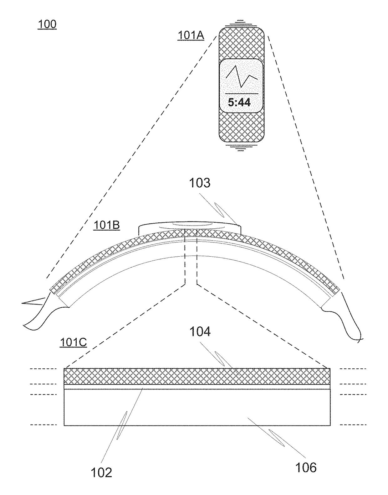
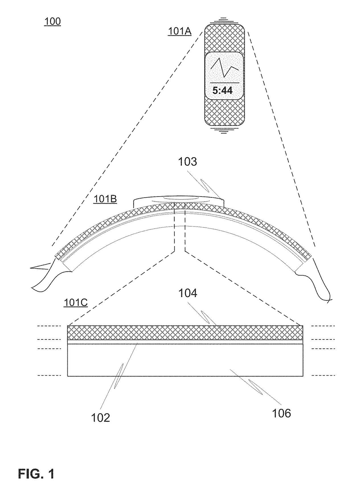
[0030]FIG. 1 illustrates, at 100, one, merely exemplary, use scenario and embodiment of the present invention wherein a curved / flexible multilayer structure has been obtained for use with an electronic product, such as armband or wristband computer, the front view of which is coarsely depicted at 101A. A person skilled in the art acknowledges the fact that the principles of the present invention may be well applied to non-curved / non-flexible substrates and constructions as well.

[0031]The target electronic product or device 101A incorporating the multilayer structure may include e.g. a consumer electronics device, industrial electronics, automation equipment, machinery, automotive product, safety or protection device, computer, tablet, phablet, mobile terminal such as cell phone, alarming device, wearable electronics / product (garment, headwear, footwear, etc.), sensor device, measurement device, display device, game controller or console, lighting device, multimedia or audio player, ...


PUM

PropertyMeasurementUnit
Lengthaaaaaaaaaa
Lengthaaaaaaaaaa
Lengthaaaaaaaaaa

Abstract

Multilayer structure (200) for electronic devices, including a flexible substrate film (102) for accommodating electronics, a number of electrical elements (204, 206) provided to the flexible substrate film, preferably by element of printed electronics and/or surface mounting, a protective layer (104) laminated onto at least first surface of the substrate film, the protective layer being configured to mask perceivable physical deviation of the substrate, such as uneven surface profile or coloring, substantially at the location of the number of elements, from outside perception, optionally visual perception and/or tactile inspection taking place via the protective layer, and plastic layer (106) molded over at least second surface of the substrate film opposite to the first surface. A corresponding method of manufacture is presented.

Description

FIELD OF THE INVENTION[0001]Generally the present invention relates to electronics. In particular, however not exclusively, the invention pertains to manufacturing a multilayer structure comprising electronics on a flexible substrate.BACKGROUND[0002]Generally there exists a variety of different multilayer structures in the context of electronics and electronic products. Multilayered solutions may be manufactured using thermoforming, molding, adhesives, heat and / or pressure based lamination, etc. In-mold decoration (IMD) / in-mold labeling (IML) may be harnessed to incorporate desired coloring and e.g. graphical patterns within the structure.[0003]The motivation or need striving for multilayer structures may be as diverse as the related use contexts. Relatively often size savings, weight savings, cost savings, or just efficient integration of components is sought for when the determined solution ultimately exhibits a multilayer nature. In turn, the associated use scenario may relate to...

Claims


Application Information

Patent Timeline
IPC IPC(8): H05K1/00H05K3/00G06F1/16B29C51/14H05K1/18B29C51/16B29L31/34
CPCB29C51/14G06F1/163G06F1/1652G06F1/1658H05K1/185H05K1/189H05K3/0014B29C51/16B29L2031/3406B29L2031/3425B29L2031/3431B29L2031/3481H05K2201/0108H05K2201/0133H05K2201/0145H05K2201/0154H05K2201/09118H05K2201/10545H05K1/0284H05K3/284H05K2203/1311H05K2203/1316H05K1/0266
Inventor NISKALA, PAAVOSAASKI, JARMORAAPPANA, PASIHEIKKINEN, MIKKOSIPPARI, MIKKOTORVINEN, JARKKOKERANEN, ANTTI
Owner TACTOTEK
Why Eureka
Try Eureka