Semiconductor integrated optical device, manufacturing method thereof and optical module

a technology of integrated optical devices and semiconductors, applied in the direction of lasers, laser details, optical waveguide light guides, etc., can solve the problems of process failure and reduce yield, and achieve the effect of increasing yield and reducing connection failur

Active Publication Date: 2017-10-03
LUMENTUM JAPAN INC
View PDF8 Cites 1 Cited by
  • Summary
  • Abstract
  • Description
  • Claims
  • Application Information

AI Technical Summary

Benefits of technology

[0017]As described above, in a semiconductor optical integrated device configured such that a first semiconductor element including an active layer and a second semiconductor element including a waveguide layer are BJ connected to each other, there has been a problem in that connection failure occurs between the semiconductor layers formed by epitaxial growth above the active layer and above the waveguide layer, which lowers the yield.
[0034]According to the semiconductor integrated optical device of the one embodiment of the present invention, the connection failure may be reduced in the vicinity of the BJ connected interface of the semiconductor regrowth layer including the etching stop layer or the diffraction grating layer, which is formed across a region above the active layer and the waveguide layer, thereby being capable of increasing the yield.

Problems solved by technology

Therefore, in the DFB laser region and the DBR mirror region, a level difference may be caused between the etching stop layers, which may allow an etchant to enter the device from the level difference to cause process failure.
As described above, in a semiconductor optical integrated device configured such that a first semiconductor element including an active layer and a second semiconductor element including a waveguide layer are BJ connected to each other, there has been a problem in that connection failure occurs between the semiconductor layers formed by epitaxial growth above the active layer and above the waveguide layer, which lowers the yield.

Method used


Image

  • Semiconductor integrated optical device, manufacturing method thereof and optical module
  • Semiconductor integrated optical device, manufacturing method thereof and optical module
  • Semiconductor integrated optical device, manufacturing method thereof and optical module

Examples


first embodiment

[0069]A first embodiment of the present invention is obtained by applying the present invention to a ridge waveguide upper diffraction grating DR laser (example of semiconductor optical integrated device) in which a DFB laser region and a DBR mirror region are BJ integrated via a side wall-shaped control layer.

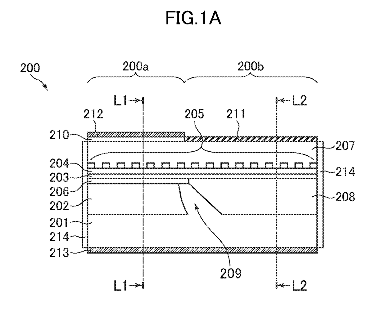
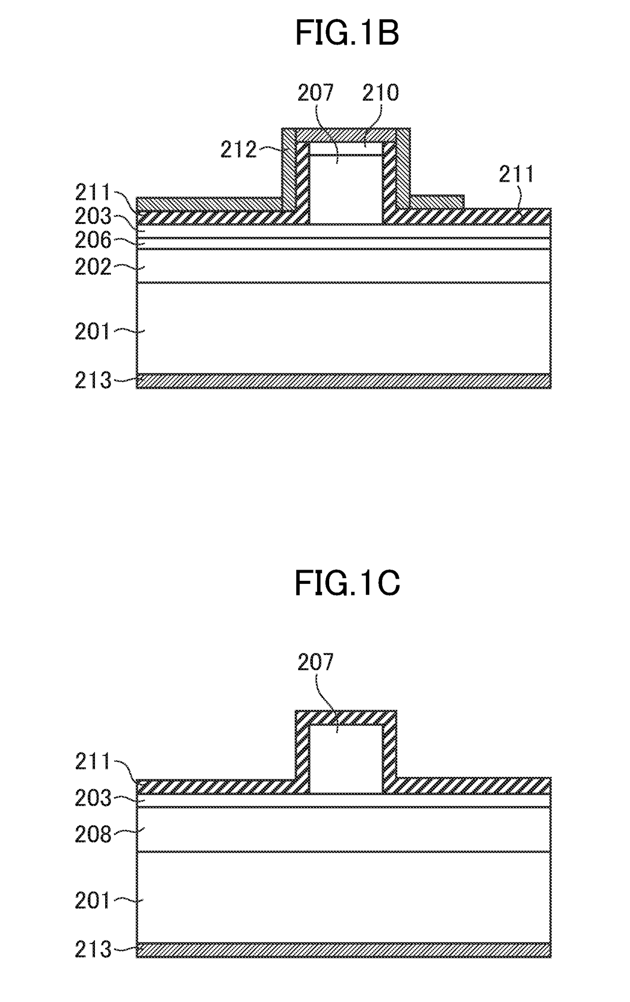
[0070]The structure of the upper diffraction grating DR laser according to the first embodiment of the present invention is described with reference to FIG. 1A, FIG. 1B, and FIG. 1C. FIG. 1A is a sectional view taken along an optical axis direction of the upper diffraction grating DR laser. Further, FIG. 1B and FIG. 1C are sectional views taken perpendicular to the optical axis direction at positions L1 and L2 in FIG. 1A, respectively.

[0071]As illustrated in FIG. 1A, a DR laser 200 according to the first embodiment includes a DFB laser region 200a to be subjected to current injection to emit light, and a DBR mirror region 200b not subjected to current injection but configured ...

second embodiment

[0105]Next, a second embodiment of the present invention is described. The second embodiment is obtained by applying the present invention to a ridge waveguide upper diffraction grating DR laser in which the DFB laser region and the DBR mirror region are BJ integrated via a side wall-shaped control layer.

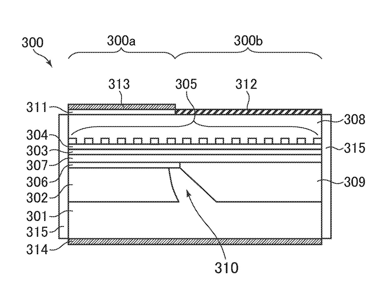
[0106]FIG. 3 is a sectional view taken along an optical axis direction of a DR laser 300 according to the second embodiment. As illustrated in FIG. 3, the DR laser 300 according to the second embodiment differs from the DR laser 200 described in the first embodiment in that the DR laser 300 includes a p-type InP buffer layer 307 in the lowermost layer of the epitaxial growth layers formed after the BJ integration. Other points are the same.

[0107]That is, in the DR laser 300 according to the second embodiment, a DFB laser region 300a includes an n-type InP substrate 301, an InGaAlAs based active layer 302, a p-type InP spacer layer 306, the p-type InP buffer layer 307, a p-type etchi...

third embodiment

[0117]Next, a third embodiment of the present invention is described. The third embodiment is an example obtained by applying the present invention to a DR laser having a horizontal oscillator surface emitting mechanism (example of surface emitting semiconductor device). FIG. 4A is a sectional view taken along an optical axis direction of a DR laser 400 according to this embodiment, and FIG. 4B is a top view thereof.

[0118]As illustrated in FIG. 4A, in the DR laser 400 according to the third embodiment, a front DBR mirror region 400a and a rear DBR mirror region 400c are respectively BJ integrated to both ends of a DFB laser region 400b via side wall-shaped control layers, and an integrated mirror 416 is integrated on the front side of the front DBR mirror region 400a. Further, an integrated lens 417 is integrated at an emitting surface that the laser light generated from the DFB laser region 400b and reflected by the integrated mirror arrives.

[0119]In the following, with reference t...


PUM


Abstract

Provided is a butt-jointed (BJ) semiconductor integrated optical device having a high manufacturing yield. A semiconductor integrated optical device, which is configured such that, on a semiconductor substrate, a first semiconductor optical element including an active layer and a second semiconductor optical element including a waveguide layer are butt-jointed to each other with their optical axes being aligned with each other, includes: a semiconductor regrowth layer including at least one of a diffraction grating layer or an etching stop layer, which is formed by one epitaxial growth across an entire surface above the active layer and the waveguide layer; and a cladding layer formed above the semiconductor regrowth layer.

Description

CROSS-REFERENCE TO RELATED APPLICATION[0001]The present application claims priority from Japanese application JP 2014-248981, filed on Dec. 9, 2014, the content of which is hereby incorporated by reference into this application.BACKGROUND OF THE INVENTION[0002]1. Field of the Invention[0003]The present invention relates to a semiconductor integrated optical device, a manufacturing method thereof, and an optical module.[0004]2. Description of the Related Art[0005]In recent years, in order to increase a device function and downsize an optical module, there has been developed a semiconductor optical integrated device in which a laser portion configured to generate light and various functional elements are monolithically integrated on the same substrate (for example, JP 2008-277445 A).[0006]As a method of manufacturing the integrated structure, there is known a method involving forming a mask in a partial region of a semiconductor laminated structure first formed by crystal growth, remo...

Claims


Application Information

Patent Timeline
Patent Type & Authority Patents(United States)
IPC IPC(8): G02B6/12H01S5/20H01S5/12H01S5/028H01S5/22H01S5/026H01S5/227H01S5/125
CPCH01S5/1231H01S5/209H01S5/0267H01S5/0287H01S5/125H01S5/22H01S5/2275
Inventor ADACHI, KOICHIROSUZUKI, TAKANORISAKUMA, YASUSHINAOE, KAZUHIKONAKANISHI, AKIRA
Owner LUMENTUM JAPAN INC
Why Eureka
Try Eureka