Method for bonding bare chip dies

a technology of bare dies and bonding methods, applied in the direction of soldering apparatus, semiconductor/solid-state device details, manufacturing tools, etc., can solve the problems of not having the necessary resolution, prone to dislocation, and suffering from certain intrinsic limitations, so as to prevent the matter of bonding

Active Publication Date: 2018-01-02
NEDERLANDSE ORG VOOR TOEGEPAST-NATUURWETENSCHAPPELIJK ONDERZOEK (TNO) +1
View PDF75 Cites 6 Cited by
  • Summary
  • Abstract
  • Description
  • Claims
  • Application Information

AI Technical Summary

Benefits of technology

[0014]Accordingly, an alternative bonding method is provided, wherein the bonding matter can be transferred with a desired resolution size, and at the same time preventing that the bonding matter be rendered ineffective by thermal overexposure in the transferring process. The bonding matter can be formed by a thermosettable or thermoplastic adhesive or by a flux containing solder paste wherein, in the transfer of the flux containing solder paste from the die bonding material to the substrate surface, the laser beam is restricted in timing and energy, in such a way that the flux remains intact within the transferred bonding matter. It is understood that the bonding matter remains intact when the bonding material keeps its bonding properties after transferring the bonding matter from the bonding material layer to the pads or pad structure, i.e. that the bonding matter remains suitable for bonding by means of the fixing step, i.e. curing the thermosetting material or reflowing the solder paste. In this way an efficient bonding method is provided wherein pads of the micro-electronic component can be bonded and electrically interconnected with resolution spot sizes that are significantly smaller than the conventional pad sizes in particular, by positioning the micro-electronic components with reference to micro-features arranged on a flexible substrate.

Problems solved by technology

The current techniques are efficient; however, they suffer from certain intrinsic limitations.
a) Screen and stencil printing are fast techniques, however they don't have the necessary resolution (100 um approx.).
The contact mode and the web movements of the substrate make it prone to dislocation.
As it is a contact mode process, damage to fragile substrates is possible and only a single layer of material can be deposited before chip placement.
It cannot handle non-flat surfaces and especially for foil based roll to roll processes web deformation cannot be compensated.
In addition, fabrication of a screen is expensive, not very flexible and they have to be replaced after 10,000 to 100,000 runs for screen printing and 200,000 for stencil printing.
Their resolution is however limited to 250 um which is not sufficient for most bare die Si chips and miniature passive components.
In addition they are relatively slow processes with typically throughputs of 10 dots per second.
c) Pintransfer is a possible method however it is restricted in viscosity range and thicknesses of the layers to be transferred and not flexible in the shapes to be transferred
However, this method is not a face down bonding method wherein electrical connections on the chip and on the substrate are pointing in the same direction and it also does not provide any fixation by adhesion to the substrate.
It is inadequate since it provides only an electrical connections after placement of the bare die in pockets on a polyimide substrate but no structural adhesion.
Moreover, this method is not suitable for most interconnect materials such as thermosettable conductive adhesives as using a laser pulse will cure or degrade the adhesive rendering it unsuited for bonding.

Method used


Image

  • Method for bonding bare chip dies
  • Method for bonding bare chip dies
  • Method for bonding bare chip dies

Examples


Embodiment Construction

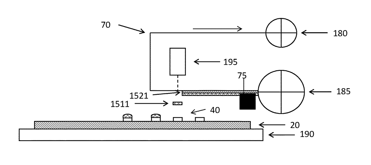
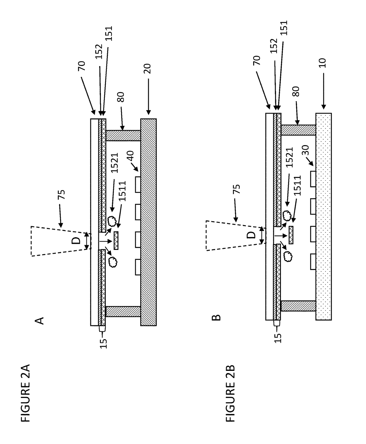
[0022]In an aspect, a direct write method is provided for high speed positioning die bonding material for discrete chip components on substrates, which can be operated in a reel to reel manufacturing fashion. In particular, the method can be used for high resolution deposition of highly viscous materials. With the attainable resolution of the disclosed methods and systems, that a resolution spot size of transferred die bonding material may be attained with a spot diameter of the transferred bonding material that is smaller than 50 micron.

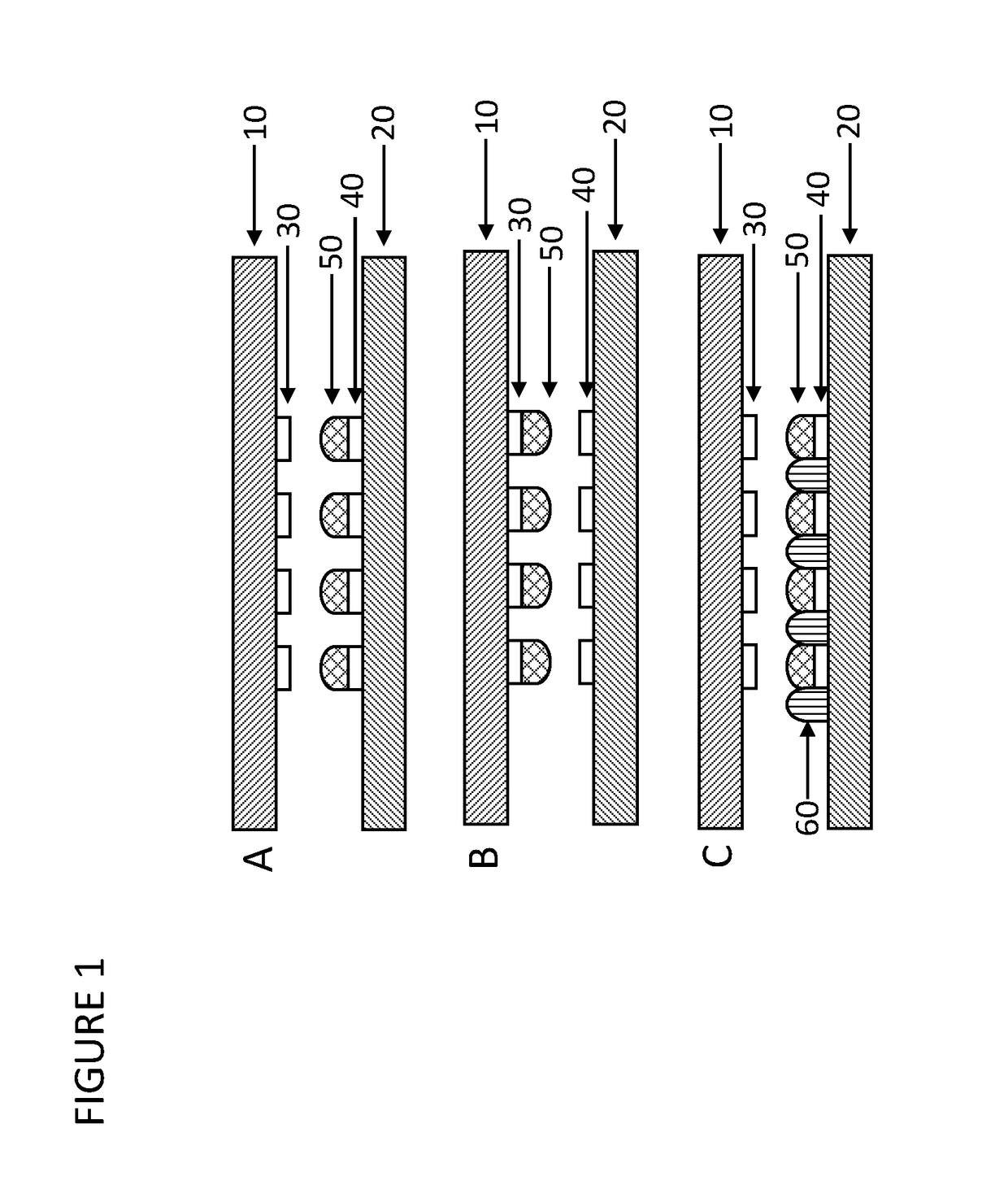
[0023]FIG. 1 illustrates schematically several embodiments (A,B,C) of methods for bonding discrete pads 30 of a bare die chip components (chips) 10 on a pad structure 40 of flexible substrate 20. As illustrated further below, the method has sufficient accuracy to correct for web deformations of the flexible substrate 20. The term “flexible substrate” used in this text refers in particular to a substrate that is bendable enough to be used in a reel t...


PUM

PropertyMeasurementUnit
operating temperatureaaaaaaaaaa
distanceaaaaaaaaaa
thicknessaaaaaaaaaa

Abstract

A method is provided for assembly of a micro-electronic component, in which a conductive die bonding material is used. This material includes a conductive thermosettable resin material or flux based solder and a dynamic release layer adjacent to the conductive thermoplastic material die bonding material layer A laser beam is impinged on the dynamic release layer, adjacent to the die bonding material layer, in such a way that the dynamic release layer is activated to direct conductive die bonding material matter towards the pad structure to be treated, to cover a selected part of the pad structure with a transferred conductive die bonding material. The laser beam is restricted in timing and energy, in such a way that the die bonding material matter remains thermosetting. Accordingly, adhesive matter can be transferred while preventing that the adhesive is rendered ineffective by thermal overexposure in the transferring process.

Description

CROSS-REFERENCE TO RELATED APPLICATIONS[0001]This application is a U.S. National Stage application under 35 U.S.C. §371 of International Application PCT / NL2013 / 050800 (published as WO 2014 / 073963 A2), filed Nov. 8, 2013, which claims priority to Application EP 12192091.2, filed Nov. 9, 2012. Benefit of the filing date of each of these prior applications is hereby claimed. Each of these prior applications is hereby incorporated by reference in its entirety.FIELD OF INVENTION[0002]The invention relates to bare die chip component interconnection and fixation method on a substrate, in particular, a flexible substrate.BACKGROUND[0003]Interconnection of discrete bare chip components or microelectronic components (chips) on a substrate is a process for which precision material deposition with sufficient accuracy is necessary to allow for miniature electrical or other type of interconnects so that when a chip component becomes attached to a placement position all electrical connection and f...

Claims


Application Information

Patent Timeline
Patent Type & Authority Patents(United States)
IPC IPC(8): H01L21/00B23K35/26H01L21/48C09J5/06B23K35/02H01L21/50H01L23/00H01L21/60H01L33/62H01L21/56H01L21/683H01L23/498
CPCH01L24/83B23K35/02B23K35/26B23K35/262C09J5/06H01L21/4853H01L21/50H01L23/49816H01L24/11H01L24/27C09J2201/61C09J2203/326C09J2205/31H01L21/563H01L21/6835H01L23/4985H01L24/13H01L24/16H01L24/73H01L24/81H01L24/92H01L33/62H01L2021/60277H01L2221/68359H01L2221/68381H01L2224/111H01L2224/11003H01L2224/1111H01L2224/1133H01L2224/13005H01L2224/13111H01L2224/14131H01L2224/27001H01L2224/29011H01L2224/29013H01L2224/29034H01L2224/73103H01L2224/73104H01L2224/742H01L2224/75252H01L2224/81191H01L2224/81192H01L2224/81815H01L2224/81862H01L2224/83192H01L2224/83224H01L2224/83862H01L2224/9211H01L2924/07802H01L2924/10253H01L2924/12042H01L2924/381H01L2224/81H01L2224/83H01L2924/2076H01L2924/01047H01L2924/01029H01L2924/00H01L2924/00012H01L2224/1329H01L2224/133C09J2301/304C09J2301/416H01L2224/27334
Inventor SMITS, EDSGER CONSTANT PIETERPERINCHERY, SANDEEP MENONVAN DEN BRAND, JEROENMANDAMPARAMBIL, RAJESHSCHOO, HARMANNUS FRANCISCUS MARIA
Owner NEDERLANDSE ORG VOOR TOEGEPAST-NATUURWETENSCHAPPELIJK ONDERZOEK (TNO)
Why Eureka
Try Eureka