Method for processing ceramic scintillator array

a technology of scintillator array and ceramics, which is applied in the field of processing or fabricating scintillator arrays, can solve the problems of scintillation (or luminescent) light, optical crosstalk between pixels, and insufficient thickness, and achieves low light transmittance, high qualified rate of product, and controlled cut quality

Inactive Publication Date: 2018-01-16
TSINGHUA UNIV +1
View PDF23 Cites 0 Cited by
  • Summary
  • Abstract
  • Description
  • Claims
  • Application Information

AI Technical Summary

Benefits of technology

[0008]The present invention has been made in order to solve the problems described above. It is an object of the present invention to provide a method for processing ceramic scintillator arrays which combines a laser cutting process with a circular diamond blade cutting process. According to the present invention, it is possible to obtain a GOS ceramic scintillator array, for example, with a controlled cut-quality, a high qualified rate of product, and a low light transmittance.
[0019]According to the present invention, the reflecting layer of the scintillator array can have a required thickness. The present invention can solve the problem that hidden cracks arise when a GOS scintillator is irradiated by laser beams of high energy, without increasing optical absorption and loss of scintillation light on end surfaces of the cuts which adversely affects light output of the scintillator. Furthermore, the present invention can promptly remove slags from surfaces of cuts such that through-cuts can be formed without being blocked and subsequent filling of light-reflective synthetic-resin cement will not be adversely affected by the slags.

Problems solved by technology

Otherwise, it is difficult to guarantee an enough thickness of the light-reflective material filled in the gap, which may cause incomplete shielding of scintillation (or luminescent) light and optical crosstalk among the pixels.
This is because the circular diamond blade should have a certain thickness to guarantee enough strength and it is difficult to reduce the blade oscillation resulted from the vibration of the cutting machine during its high-speed rotation to a low enough extent.
However, the diamond wire saw has a complicated structure, and its processing efficiency is low for small-batch and medium-batch processing.
If the residual coolants have not been thoroughly removed and an optical synthetic-resin cement comprising titanium dioxide light-reflective powder is filled into the narrow gaps, the strength of adhesion between the scintillator pixels and the synthetic-resin cement may not be large enough.
Therefore, in this case, it is needed to pay more attention to subsequent coupling operations of the scintillator array in order to avoid fracture at the adhesive gap when the scintillator array is in a stressed state, which would increase the operation complexity.
However, there are several problems in the laser cutting for GOS scintillator.
For example, hidden cracks may arise when a GOS scintillator is irradiated by laser beams of high energy.
If a cut is not well protected during the cutting process, the cut will be blackened and thus loss of scintillation light on end surfaces of the cut will be increased, which will adversely affect light output of the scintillator.
In addition, if the slags are not promptly removed from surfaces of the cuts, the cuts will be blocked, and the non-through cuts will affect the subsequent filling of the light-reflective synthetic-resin cement.

Method used


Image

  • Method for processing ceramic scintillator array
  • Method for processing ceramic scintillator array
  • Method for processing ceramic scintillator array

Examples


Embodiment Construction

[0027]The present invention will be described below in detail with reference to the drawings.

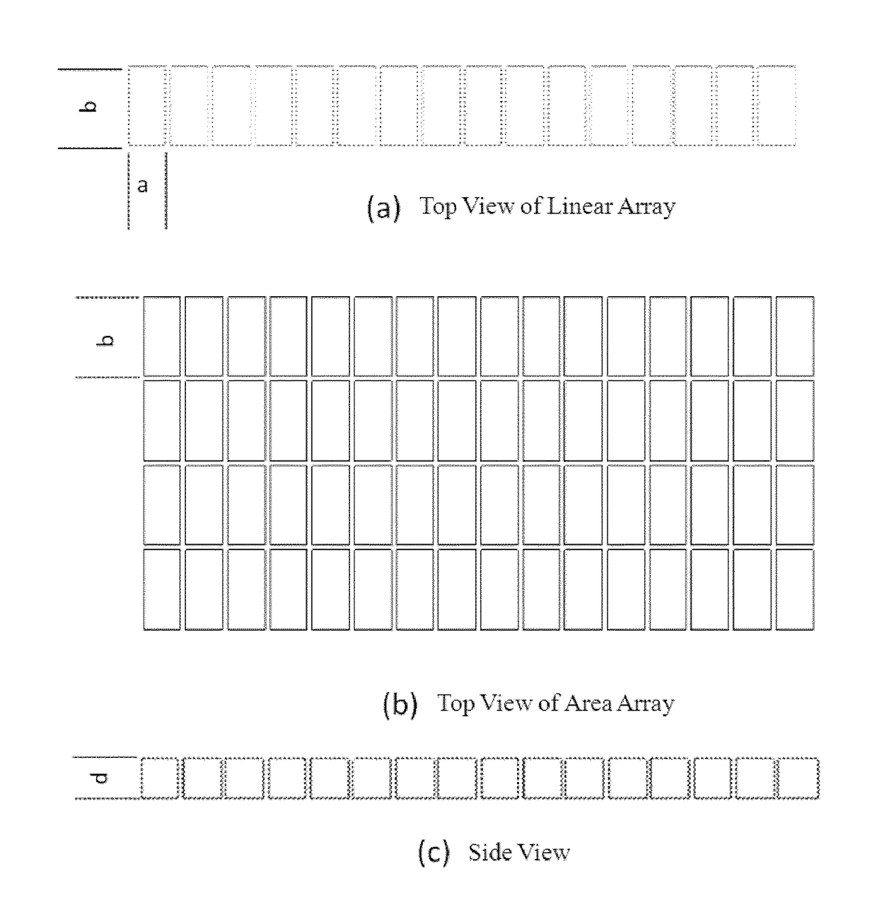
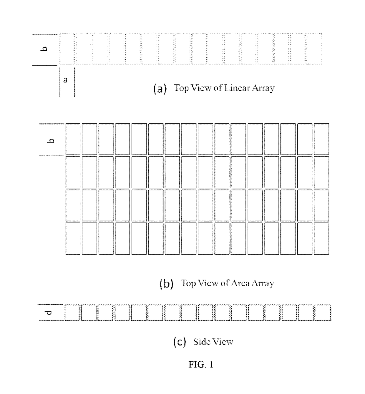
[0028]The present invention employs GOS ceramic scintillators prepared for example by means of a hot-pressing hot-isostatic-pressing two-step sintering process or a spark-plasma hot-isostatic-pressing two-step sintering process. The GOS ceramic scintillator has a density over 99% of its theoretical density and a particle size between 100 μm and 100 μm. When the GOS ceramic scintillator is made with a thickness of 1 mm, its integrated transmittance is 25-50%. However, the present invention is not limited to the GOS ceramic scintillators made by the above processes, but can also employ GOS ceramic scintillators made by other processes (for example, a spark-plasma one-step sintering process and the like). Furthermore, in order to improve efficiency of manufacture by sintering, a thickness of an initial ceramic material block is generally several times a thickness of a scintillator for practical...


PUM

PropertyMeasurementUnit
light transmittanceaaaaaaaaaa
thicknessaaaaaaaaaa
transmittanceaaaaaaaaaa

Abstract

A method for processing a ceramic scintillator array, characterized in that, comprising the following steps: (a) forming, in a first direction, a predetermined number of straight first-direction through-cuts which are parallel to each other and spaced from each other on a scintillator substrate by using laser; (b) adequately filling the first-direction through-cuts with an adhesive and solidifying the adhesive; (c) forming, in a second direction. a predetermined number of second direction through-cuts which are parallel to each other at a predetermined interval on the scintillator substrate by using laser, wherein the second direction is perpendicular to the first direction; and (d) adequately filling the second direction through-cuts with the adhesive and solidifying the adhesive bond.

Description

CROSS-REFERENCE TO RELATED APPLICATION(S)[0001]This application claims priority to Chinese Patent Application No. 201410831981.4, filed Dec. 29, 2014, published as CN 105798466 A, and entitled “Method for Processing Ceramic Scintillator Array”, which is hereby incorporated by reference in its entirety.BACKGROUND[0002]Field[0003]The present invention relates to a method for processing or fabricating a scintillator array, and more specifically to a method for fabricating, e.g., a gadolinium oxysulfide (GOS) ceramic scintillator array by using a laser cutting process and a diamond blade cutting process. The GOS scintillator array manufactured by the processing method of the present invention can be used in X-ray or γ-ray ionizing radiation imaging detectors for X-ray computed tomography (X-CT) and / or line-scan imaging, and is especially applicable to the field of radiation imaging security check.[0004]Description of Related Information[0005]A detector used in computed tomography (CT) s...

Claims


Application Information

Patent Timeline
Patent Type & Authority Patents(United States)
IPC IPC(8): G01T1/202G01T1/20
CPCG01T1/2018G01T1/20183G01T1/20185
Inventor WANG, YANCHUNZHANG, QINGJUNLI, YUANJINGCHEN, ZHIQIANGZHAO, ZIRANLIU, YINONGLIU, YAOHONGCHANG, JIANPINGZHANG, WENJIANZHAO, SHUQINGZOU, XIANGWANG, YONGQIANG
Owner TSINGHUA UNIV
Why Eureka
Try Eureka