Electronic circuit comprising a current conveyor arranged with an anti-saturation device and corresponding device for detecting photons

a current conveyor and photon detection technology, applied in the field of microelectronics and optoelectronics, can solve the problems of obtaining high amplification, giving an imperfect copy of the current coming from the detector, falsifying the measurement of amplitude, etc., to achieve the effect of optimizing temporal precision, minimizing parasitic capacitance, and facilitating the differentiation of signals

Inactive Publication Date: 2018-04-03
CENT NAT DE LA RECHERCHE SCI
View PDF5 Cites 0 Cited by
  • Summary
  • Abstract
  • Description
  • Claims
  • Application Information

AI Technical Summary

Benefits of technology

[0017]Thus, even when the intensity of the current is high, the circuit is not saturated and makes it possible, through its behavior, to make precise measurements via said first and second voltage outputs.
[0018]In particular, when the intensity of the input current is correlated with the photons received via a photomultiplier device, it is possible to make precise measurements, whatever the intensity of the input current, on data pertaining to the time of arrival of the photons, as well as the level of energy received.
[0021]Thus, such a circuit has a simple architecture that enables the current conveyor not to get saturated and therefore to provide an output current that is always identical to the input current, even for the strongest signals, ensuring the precision of the measurement of charge. It averts the use of current mirror circuits making copies of current that are not necessarily identical and having greater electronic noise. In addition such a circuit, by its simplicity (few components are needed to make the circuit) enables measurements of interest (with regard to the time of arrival of the photons and received energy levels) to be made more rapidly than with the prior-art techniques with a bandwidth greater than one GHz.
[0023]According to one particular aspect of the invention, said ratio is a real number included in the interval [10; 20]. This ratio provides for maximum amplification for the small signals corresponding to the first photons received and therefore makes it easier to distinguish these signals, thus optimizing the temporal precision.
[0024]According to one particular aspect of the invention, such an electronic circuit comprises a first resistor having a value of 100 ohms, and a second resistor having a value of 1000 ohms. These values make it possible, in integrated technology, to minimize the parasitic capacitances while at the same time providing high amplification. Such a circuit makes it possible to attain a bandwidth greater than one GHz.
[0025]According to one particular aspect of the invention, said anti-saturation device is a diode. This non-linear device has very high (logarithmic) compression on a very great dynamic range while at the same time minimizing the parasitic capacitance which limits the bandwidth, which is essential to the precise measurement of time (<10 ps)

Problems solved by technology

One difficulty encountered with current conveyors however is that of obtaining high amplification while at the same time appropriately processing the strongest signals which tend to saturate the amplifier and therefore falsify the measurement of amplitude.
However, one drawback of this first technique is that the “high gain” mirror arm which gets saturated causes distortion in the “low gain” arm and therefore gives an imperfect copy of the current coming from the detector.
In addition, these mirrors add parasitic capacitances which, at low power, reduce the bandwidth.
Finally, the current copies increase the consumption of the circuit.

Method used


Image

  • Electronic circuit comprising a current conveyor arranged with an anti-saturation device and corresponding device for detecting photons
  • Electronic circuit comprising a current conveyor arranged with an anti-saturation device and corresponding device for detecting photons
  • Electronic circuit comprising a current conveyor arranged with an anti-saturation device and corresponding device for detecting photons

Examples


first embodiment

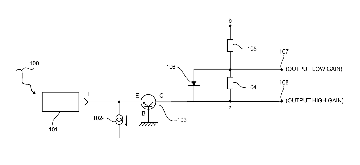
[0039]FIG. 1 presents an electronic circuit according to the invention, in which the current conveyor comprises an NPN type bipolar transistor.

[0040]When a photon is received 100 by a photomultiplier device photomultiplier 101, the current i induced by such a device is generally not intense enough to be capable of being measured by classic measurement devices. The circuit of FIG. 1 amplifies the received current while at the same time being capable of dealing with situations where a major flux of photons is received by the photomultiplier device 101.

[0041]Such a circuit has an NPN bipolar transistor 103 (i.e a current conveyor) mounted so that the base B is connected to a DC voltage source (“common base” mounting) , the collector C is connected to an active load possessing the two terminals a and b, and the emitter E is connected to the output of the photomultiplier device 101 and a biasing device 102 (which is a current source).

[0042]According to this embodiment, such an active loa...

second embodiment

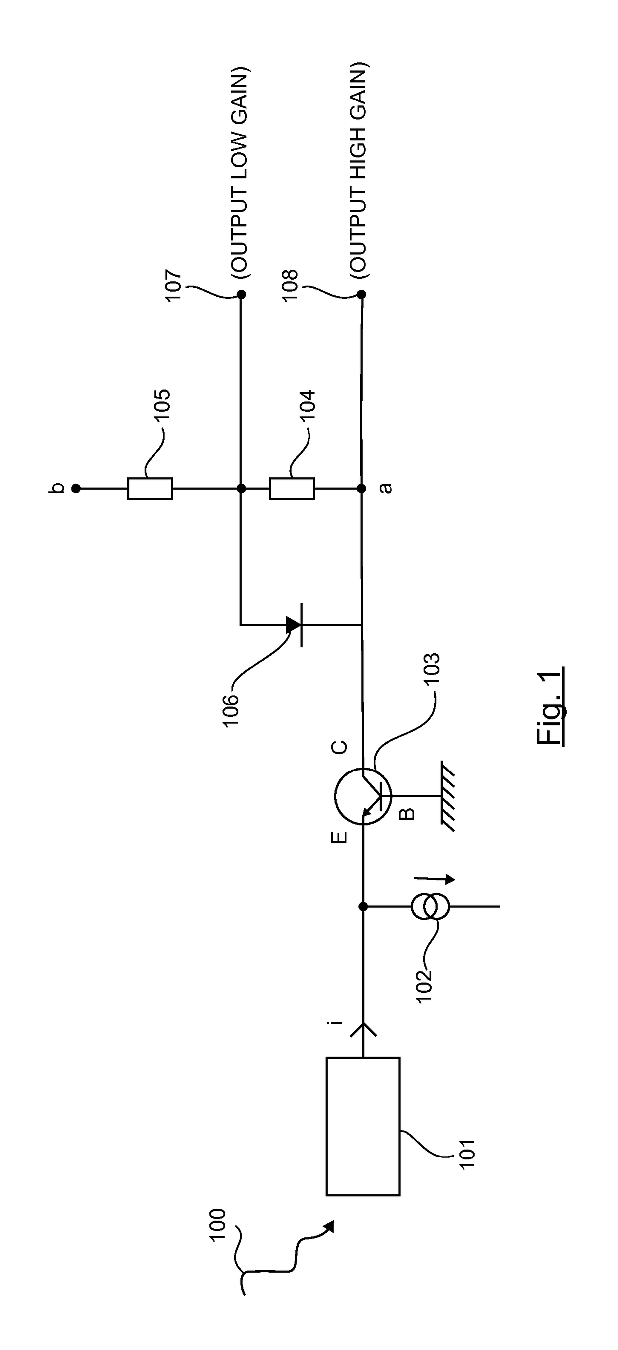
[0046]FIG. 2 presents an electronic circuit according to the invention, in which a current conveyor comprises a PNP type bipolar transistor.

[0047]In this embodiment, the current conveyor correspond to a PNP type bipolar transistor mounted so that the base B′ is connected to the ground, the collector C′ is connected to an active load possessing the two terminals a and b, and the emitter E′ is connected to the output of the photomultiplier device 101 and of a biasing device 201.

[0048]In another embodiment, the PNP type bipolar device is replaced by a PMOS transistor.

third embodiment

[0049]FIG. 3 presents an electronic circuit according to the invention, in which a current conveyor is formed by a composite mounting of two “super common base” NPN transistors.

[0050]In this embodiment, the current conveyor corresponds to the combination of two NPN transistors 302, 303 mounted so that the emitter E of the NPN type bipolar transistor 302 is connected to the ground, the collector C of the NPN type bipolar transistor 302 is connected to the base of the NPN type bipolar transistor 303, and to a biasing device 304, and the base B of the NPN type bipolar transistor 302 is connected to the emitter E of the NPN type bipolar transistor 303, the output of the photomultiplier device 101, and to a biasing device 301.

[0051]In another embodiment, such a current conveyor can also be made with combinations of NPN, NMOS, PNP or PMOS transistors.

[0052]In a preferred embodiment of the invention, the resistor 104 has a value of 1000 ohms and the resistor 105 has a value of 100 ohms.

[00...


PUM


Abstract

An electronic circuit including a current conveyor connected to a load is provided. The load delivers at least one first voltage output and one second voltage output. Such a circuit is noteworthy in that the second voltage output has what is called a non-linear behavior relative to the magnitude of the input current of the electronic circuit in a given range.

Description

1. CROSS-REFERENCE TO RELATED APPLICATION[0001]This Application is a Section 371 National Stage Application of International Application No. PCT / EP2013 / 066937, filed Aug. 13, 2013, the content of which is incorporated herein by reference in its entirety, and published as WO 2014 / 027001 on Feb. 20, 2014, not in English.2. FIELD OF THE INVENTION[0002]The field of the invention is that of microelectronics and optoelectronics.[0003]More specifically, the invention pertains to a technique concerning the current conveyors used in numerous devices capable of detecting physical parameters related to the photons received.[0004]The invention has numerous applications, for example in the medical field (and more particularly in devices used to carry out positron emission tomography (PET) as well as in fields using photomultipliers or comparable devices.3. TECHNOLOGICAL BACKGROUND[0005]We shall strive especially here below in this document to describe the problems and issues existing in the fiel...

Claims


Application Information

Patent Timeline
Patent Type & Authority Patents(United States)
IPC IPC(8): G01J1/44G01T1/17
CPCG01J1/44G01T1/17G01J2001/444
Inventor DE LA TAILLE, CHRISTOPHE
Owner CENT NAT DE LA RECHERCHE SCI
Why Eureka
Try Eureka