
Circuit module

a technology of circuit modules and circuit substrates, applied in the direction of printed circuits stress/warp reduction, printed circuit non-printed electric components association, semiconductor/solid-state device details, etc., can solve the problems of failure of mobile terminals, peeled mounting electrodes from circuit substrates, etc., to prevent the electrical characteristics of circuit modules from being deteriorated, prevent a break, a chip, or a crack from occurring in the circuit substrates.

Active Publication Date: 2018-05-01
MURATA MFG CO LTD
View PDF34 Cites 0 Cited by
  • Summary
  • Abstract
  • Description
  • Claims
  • Application Information

AI Technical Summary

Benefits of technology

The present invention provides a technology to prevent breakages, chips, or cracks in a circuit substrate and secure the electrical characteristics of a circuit module even if a portion of the mounting electrode is peeled from the circuit substrate. In addition, the invention also includes a structure to maintain the electrical connection state between the mounting electrode and the via conductor, preventing deterioration in the circuit module's electrical characteristics. An insulation layer is further included to improve the strength of the circuit substrate and prevent a break, chip, or crack from occurring in the circuit substrate. The mounting electrode is preferably placed on a diagonal line on the circuit substrate to effectively reduce concentration of stress and prevent breakage, chip, or crack from occurring in the circuit substrate.

Problems solved by technology

With the progress of the miniaturization of mounting electrodes formed on a circuit substrate included in a circuit module in this way, there is a possibility that torsion or a stress is concentrated in a portion on which a mounting electrode in the circuit substrate configuring the circuit module is formed, and a break, a chip, a crack, or the like occurs in the circuit substrate, the torsion being applied to the circuit substrate when the circuit module is mounted on the mother substrate or the like at the time of the assembly of a mobile terminal, the stress being due to an impact or the like occurring, for example, when a mobile terminal has fallen that includes a mother substrate on which the circuit module is mounted via solder or the like.
Therefore, there is a possibility that a mounting electrode is peeled from the circuit substrate.
In this way, when a break, a chip, or a crack has occurred in the circuit substrate or a mounting electrode has been peeled from the circuit substrate, a via conductor in the circuit substrate or a transmission line such as a wiring pattern formed within the circuit substrate is damaged, and hence, there is a possibility that a failure of the mobile terminal is caused.

Method used


Image

  • Circuit module
  • Circuit module
  • Circuit module

Examples


first preferred embodiment

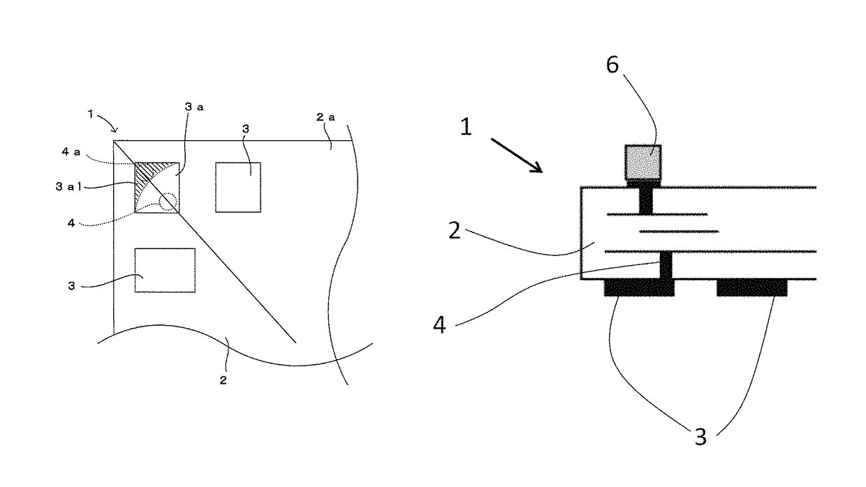
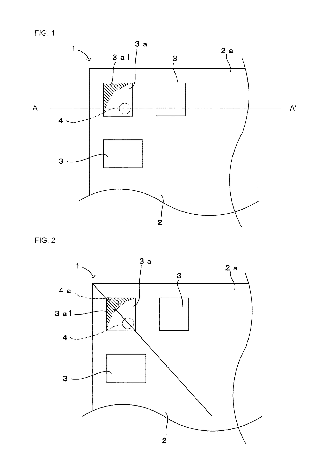
[0024]A first preferred embodiment of a circuit module of the present invention will be described with reference to FIG. 1. FIG. 1 is a main portion enlarged view of a bottom surface, which illustrates the first preferred embodiment of the circuit module of the present invention.

[0025]A circuit module 1 illustrated in FIG. 1 and FIG. 6 includes a circuit substrate 2 including a ceramic multilayer substrate where an electronic component 6, which may be a semiconductor element such as, for example, an amplifier including a transistor or an FET, a diode, or a switch or a component such as a resistance element, a capacitor element, or an inductor element is mounted on at least the front surface (the other main surface) of the ceramic multilayer substrate and land-shaped surface mounting electrodes 3 and 3a are provided on a back surface 2a (one main surface) thereof, and the circuit module 1 is configured as a module, examples of which include a Bluetooth module (registered trademark), ...

second preferred embodiment

[0034]A second preferred embodiment of the circuit module of the present invention will be described with reference to FIG. 2. FIG. 2 is the main portion enlarged view of a bottom surface, which illustrates the second preferred embodiment of the circuit module of the present invention.

[0035]This preferred embodiment is different from the above-mentioned first preferred embodiment in that, as illustrated in FIG. 2, another via conductor 4a is further connected to a position located closer to the corner portion of the circuit substrate 2, in the mounting electrode 3a in the vicinity of the corner portion of the circuit substrate 2. Since the other configuration is the same as the above-mentioned first preferred embodiment, the same symbol is assigned, and hence, the description of the configuration will be omitted.

[0036]According to this preferred embodiment, in the mounting electrode 3a in the vicinity of the corner portion of the circuit substrate 2, the other via conductor 4a is fu...

third preferred embodiment

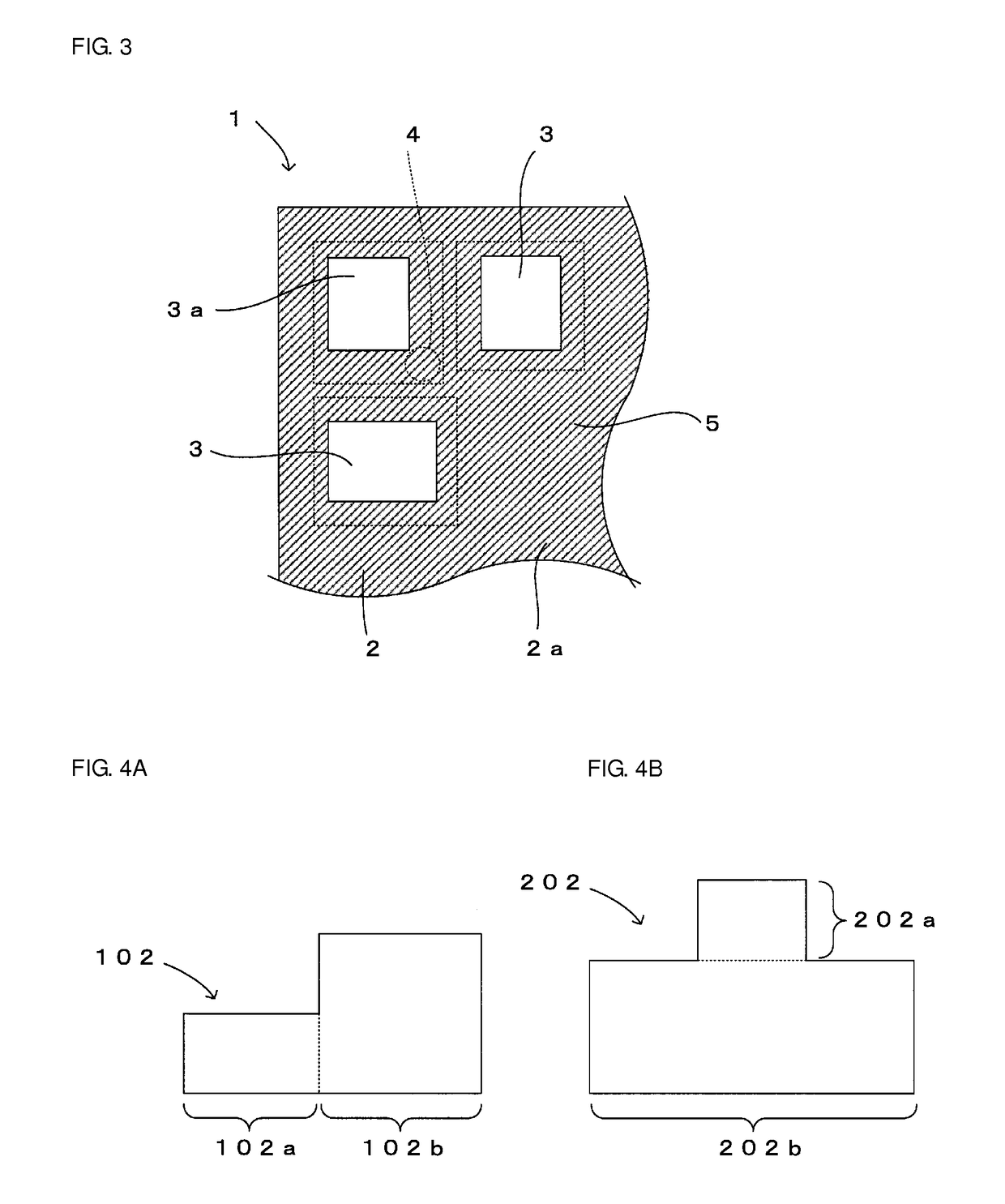
[0038]A third preferred embodiment of a circuit module of the present invention will be described with reference to FIG. 3. FIG. 3 is the main portion enlarged view of a bottom surface, which illustrates the third preferred embodiment of the circuit module of the present invention.

[0039]This preferred embodiment is different from the above-mentioned first preferred embodiment in that, as illustrated in FIG. 3, an insulation layer 5 provided on the back surface 2a of the circuit substrate 2 is further included and the insulation layer 5 is arranged to cover the circumferential portions of the individual mounting electrodes 3 and 3a. In addition, the insulation layer 5 is formed using a commonly-used resist material such as a thermosetting epoxy resin, or a ceramic paste. Since the other configuration is preferably the same or substantially the same as the above-mentioned first preferred embodiment, the same symbol is assigned, and hence, the description of the configuration will be o...


PUM


Abstract

A via conductor connected to a mounting electrode near a corner portion of a circuit substrate is provided in a position in a corresponding mounting electrode, located closer to the center of the circuit substrate. Thus, concentration of a stress in a portion of the via conductor is effectively reduced, and a break, a chip, or a crack is prevented from occurring to the circuit substrate. Even if the portion located closer to the corner portion of the mounting electrode is peeled from the circuit substrate, the electrical characteristics of the circuit module are secured because disconnection between the corresponding mounting electrode and the via conductor is prevented.

Description

BACKGROUND OF THE INVENTION[0001]1. Field of the Invention[0002]The present invention relates to a circuit module including a circuit substrate in which a plurality of land-shaped mounting electrodes are provided on one main surface.[0003]2. Description of the Related Art[0004]In recent years, further downsizing of mobile terminals has been desired, and further miniaturization and further lowering of heights of circuit modules (high-frequency electronic modules) to be mounted on the mother substrates or the like of mobile terminals has been requested, examples of the circuit modules including a Bluetooth module (registered trademark), a wireless LAN module such as WiFi, and an antenna switch module used for a cellular phone. Such a circuit module includes a circuit substrate where a semiconductor element such as a transistor, an FET, a diode, or an IC or a component such as a resistance element, a capacitor element, or an inductor element is mounted on the front surface of the circu...

Claims


Application Information

Patent Timeline
Patent Type & Authority Patents(United States)
IPC IPC(8): H05K1/00H05K1/11H01L23/498H05K1/02H05K1/18H05K7/06H05K3/46
CPCH05K1/0271H01L23/49827H01L23/49838H05K1/113H05K1/181H05K7/06H01L2924/0002H05K2201/09381H05K3/4629H05K2201/099H05K2201/0979H01L2924/00
Inventor KITAJIMA, HIROMICHI
Owner MURATA MFG CO LTD
Learn More