Etching method and etching apparatus

a technology of etching apparatus and cobalt film, which is applied in the manufacture of printed circuits, basic electric elements, solid-state devices, etc., can solve the problem of the formation of carbon films, and achieve the effect of suppressing the decomposition of etching gas

Active Publication Date: 2018-06-05
TOKYO ELECTRON LTD +1
View PDF12 Cites 205 Cited by
  • Summary
  • Abstract
  • Description
  • Claims
  • Application Information

AI Technical Summary

Benefits of technology

[0009]In accordance with a second aspect of the present invention, there is provided an etching method including: supplying a target object with an oxidizing gas to oxidize a cobalt film formed on a surface of the target object; and etching the oxidized cobalt film by supplying an etching gas containing β-diketone and a decomposition suppressing gas for suppressing decomposition of the etching gas.

Problems solved by technology

Since the wet etching is not suitable for controlling the etching with high accuracy, it is considered to etch the Co film by using a gas.
Japanese Patent Application Publication No. 2015-12243 discloses that the O2 gas and the Hfac gas are simultaneously supplied to the wafer while heating the substrate to a comparatively high temperature ranging from 300° C. to 400° C. In that case, the carbon film is formed; however, Japanese Patent Application Publication No. 2015-12243 does not pay attention to the formation of the carbon film by the Hfac gas, and cannot solve the problem of the formation of the carbon film.

Method used


Image

  • Etching method and etching apparatus
  • Etching method and etching apparatus
  • Etching method and etching apparatus

Examples


first embodiment

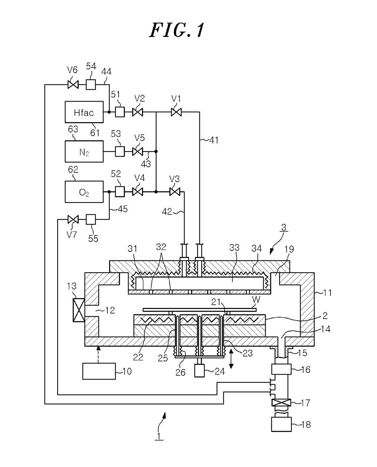
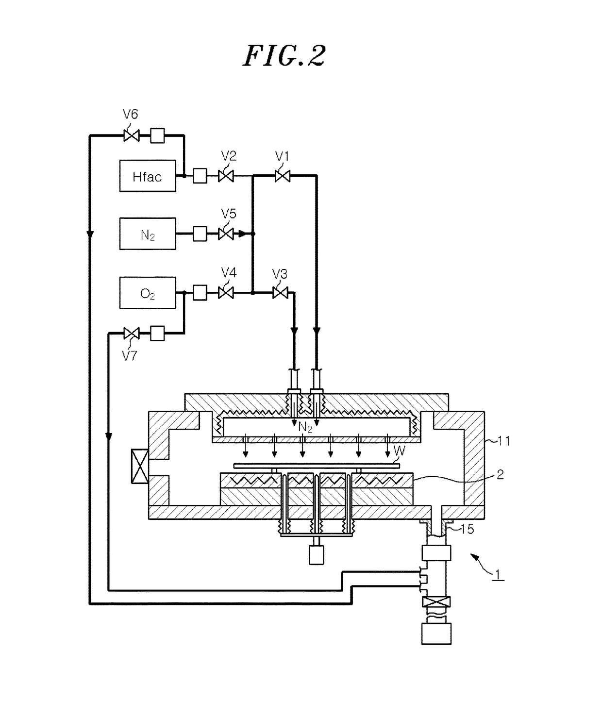
[0022]An etching apparatus 1 for performing an etching method according to a first embodiment will be described with reference to FIG. 1. A cobalt (Co) film for forming a wiring of a semiconductor device is formed on a surface of a wafer W as a target object to be processed by the etching apparatus 1. The etching apparatus 1 includes a processing chamber 1 that is a vacuum chamber having an approximately circular cross sectional shape. A reference numeral 12 in the drawing indicates a loading / unloading port that is opened at a side surface of the processing chamber 11 to load and unload the wafer W. The loading / unloading port 12 is opened / closed by a gate valve 13. A heater (not shown) for heating an inner surface of the processing chamber 11 to a predetermined temperature is provided at the processing chamber 11.

[0023]A cylindrical stage 2, on which the wafer W is mounted, is provided in the processing chamber 11. Reference numeral 21 in the drawing indicates supporting pins for su...

second embodiment

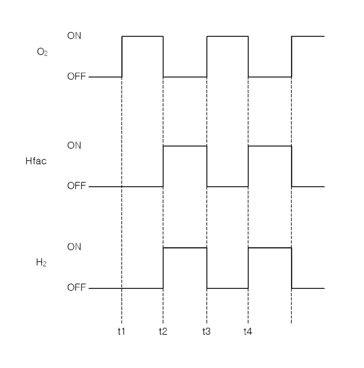
[0039]Hereinafter, an etching apparatus 7 for performing an etching method according to a second embodiment will be described with reference to FIG. 4. Here, the difference between the etching apparatus 1 and the etching apparatus 7 will be described mainly. The etching apparatus 7 has a gas supply line 46 having a downstream end opened to the dispersion space 33 and an upstream end connected to an H2 gas supply source 64 for suppressing decomposition of the Hfac gas via valves V8 and V9 and a flow rate controller 56 in that order.

[0040]An upstream end of a bypass line 47 is connected to a position between the H2 gas supply source 64 and the flow rate controller 56 in the gas supply line 46. A downstream end of the bypass line 47 is connected to a position between the pressure control valve 16 and the opening / closing valve 17 in the gas exhaust line 15 via a flow rate controller 57 and a valve V10 in that order. Similar to the bypass lines 44 and 45, the bypass line 47 is used for s...


PUM

PropertyMeasurementUnit
temperatureaaaaaaaaaa
distanceaaaaaaaaaa

Abstract

An etching method includes a step of etching a cobalt film formed on a surface of a target object by supplying an etching gas containing β-diketone and an oxidizing gas for oxidizing the cobalt film to the target object. The supply of the etching gas and the oxidizing gas is carried out such that a flow rate ratio of the oxidizing gas to the etching gas is ranging from 0.5% to 50% while heating the target object to a temperature lower than or equal to 250° C.

Description

CROSS-REFERENCE TO RELATED APPLICATION[0001]This application claims priority to Japanese Patent Application No. 2015-147846 filed on Jul. 27, 2015, the entire contents of which are incorporated herein by reference.FIELD OF THE INVENTION[0002]The disclosure relates to an etching method and an etching apparatus for a cobalt film.BACKGROUND OF THE INVENTION[0003]A cobalt silicide (CoSi2) layer may be formed by depositing a cobalt (Co) film on a silicon (Si) film as a wiring of a semiconductor device and heating the Co film. After the CoSi2 layer is formed, a semiconductor wafer (hereinafter, referred to as “wafer”) that is a substrate on which the CoSi2 layer is formed is immersed in a liquid chemical and subjected to wet etching. Accordingly, a residual Co film is completely removed.[0004]Along with the trend toward miniaturization of semiconductor devices, it is considered to use Co as a wiring instead of Cu (copper) that has been conventionally used as a wiring. This is because when...

Claims


Application Information

Patent Timeline
Patent Type & Authority Patents(United States)
IPC IPC(8): H01L21/67H01L21/311H01L21/3213H01L21/3065H05K3/02H01L23/532
CPCH01L21/67069H01L21/3065H01L21/31116H01L21/31138H01L21/32135H05K3/02H01L21/32136H05K2203/0315H01L21/32138H01L23/53209H01L2924/01027C23F1/12H01L21/02175H01L21/02244H01L21/31122H01L21/324H01L21/67098
Inventor LIN, JUNTAKEYA, KOJITACHIBANA, MITSUHIROYAO, AKIFUMIYAMAUCHI, KUNIHIROMIYAZAKI, TATSUO
Owner TOKYO ELECTRON LTD
Why Eureka
Try Eureka