

Semiconductor laser device and method of manufacturing the semiconductor laser device
a laser device and semiconductor technology, applied in semiconductor lasers, laser optical resonator construction, laser details, etc., can solve the problem of reducing thickness of portions, affecting the effect of preventing substrate breakage and reducing thickness
- Summary
- Abstract
- Description
- Claims
- Application Information
AI Technical Summary
Benefits of technology
Problems solved by technology
Method used
Image

Examples
first embodiment
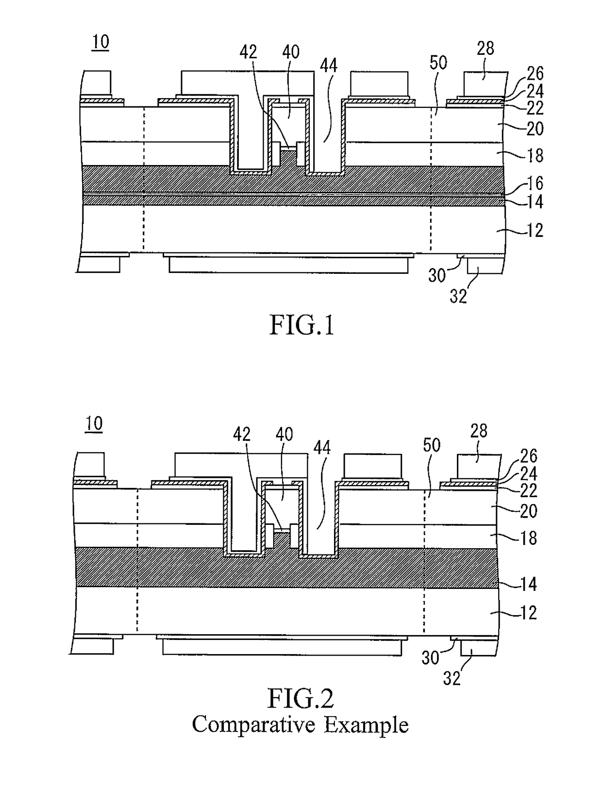
[0020]FIG. 1 is a sectional view of a semiconductor laser device in a wafer state. This semiconductor laser device in a wafer state is divided along broken lines in the future. The semiconductor laser device has a substrate 12 formed of InP and a buffer layer 14 formed of InP provided on an upper surface of the substrate 12. The buffer layer 14 is partitioned into an upper portion and a lower portion by an epi intermediate layer 16 formed in the buffer layer 14.
[0021]The material of the epi intermediate layer 16 is a compound semiconductor containing As. For example, the material of the epi intermediate layer 16 is InGaAsP, AlGaInAs, AlInAs or InGaAs. These compound semiconductors can be easily lattice-matched to the buffer layer 14 formed of InP.
[0022]A plurality of laser elements having a ridge structure are formed above the buffer layer 14. Each laser element is, for example, a DFB laser element. The structure of the laser element will be described. A block layer 18 formed of InP...
second embodiment
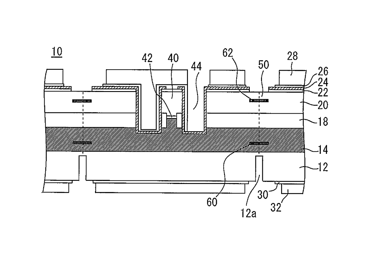
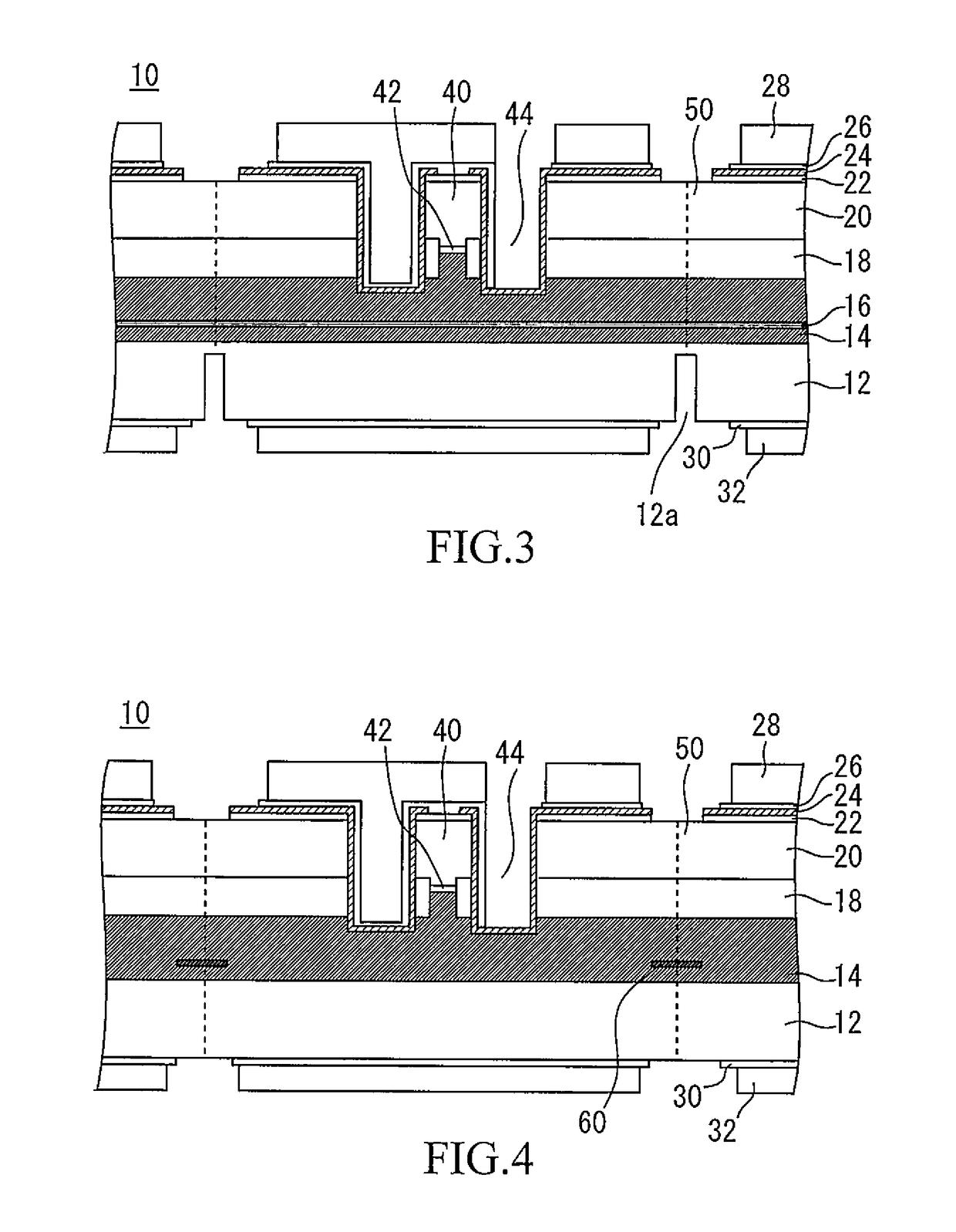
[0034]FIG. 3 is a sectional view of the semiconductor laser device in a wafer state according to the second embodiment. Grooves 12a are formed in the lower surface of the substrate 12 in separating sections 50. Each groove 12a may be stitch grooves (grooves intermittently formed) or a continuous groove (a groove continuously formed). It is preferable that the grooves 12a have a width which allows a scribing blade to enter the groove, and which is about ⅙ of the chip width. The depth of the grooves 12a is not particularly specified if the grooves 12a do not reach the epi intermediate layer 16. The depth of the grooves 12a is, for example, several microns to several tens of microns.
[0035]It is desirable to form the grooves 12a by dry etching using a novolak-based negative resist mask or an insulating film hard mask capable of maintaining a high resist selectivity and using a kind of chlorine-based gas. The grooves 12a are formed before the chip producing step.
[0036]In the chip produci...
third embodiment
[0037]FIG. 4 is a sectional view of the semiconductor laser device in a wafer state according to the third embodiment. An epi intermediate layer 60 is provided only in the separating sections 50 by avoiding positions right below the ridge structures 40. An epi intermediate layer is formed on the entire area of the buffer layer 14 and unnecessary portions thereof are thereafter removed by etching, thus obtaining the epi intermediate layer 60. Since the epi intermediate layer 60 is provided in each separating section 50, the substrate can easily be divided in the chip producing step.
[0038]In the first and second embodiments, the epi intermediate layer 16 is formed through the entire semiconductor device, therefore it is necessary to increase the thickness of the buffer layer 14 to such an extent that the epi intermediate layer 16 does not interfere with the distribution of the intensity of light from the active layer. Forming the thick buffer layer 14 requires a long epi growth time. ...
PUM
 Abstract
Description
Claims
Application Information