

Compact programmable photonic variable delay devices
- Summary
- Abstract
- Description
- Claims
- Application Information
AI Technical Summary
Benefits of technology
Problems solved by technology
Method used
Image

Examples
Embodiment Construction
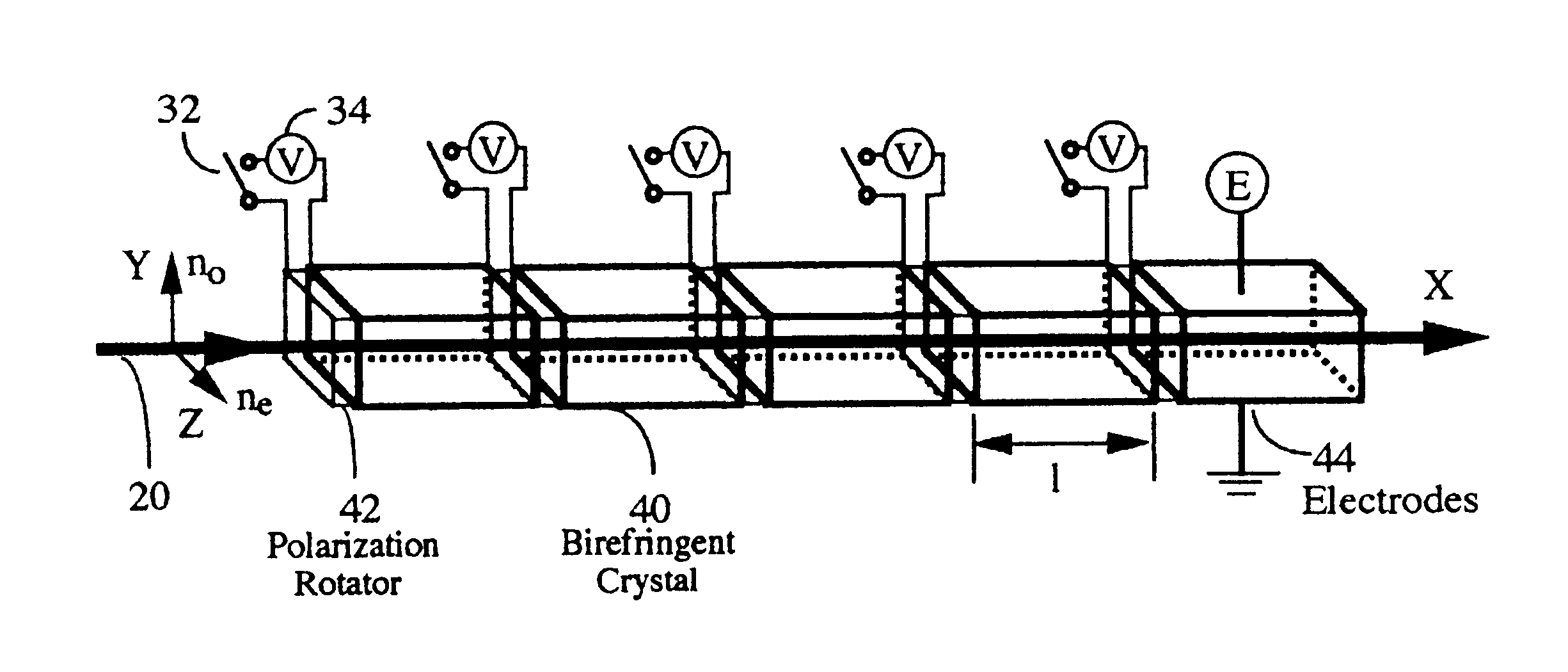
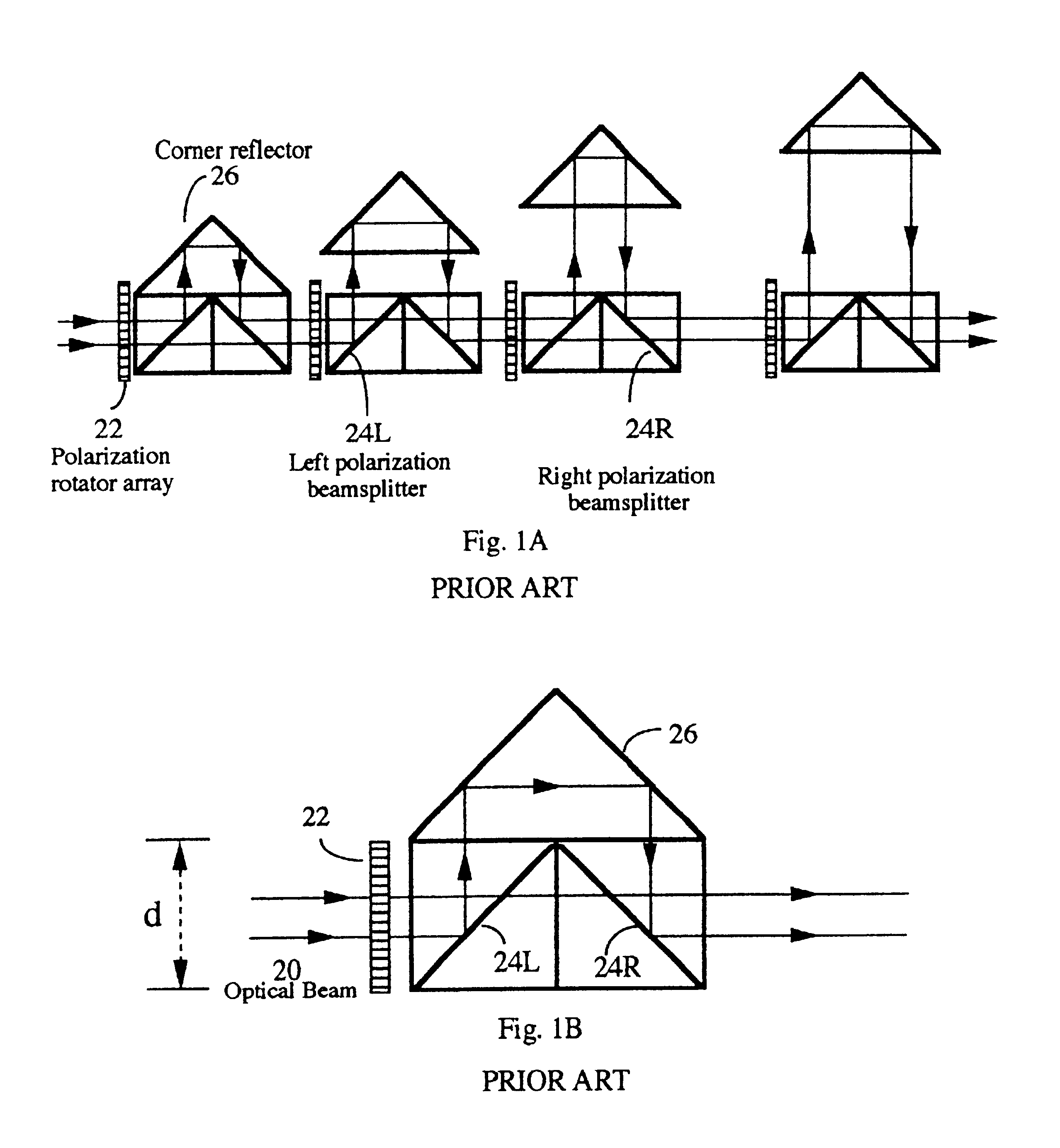
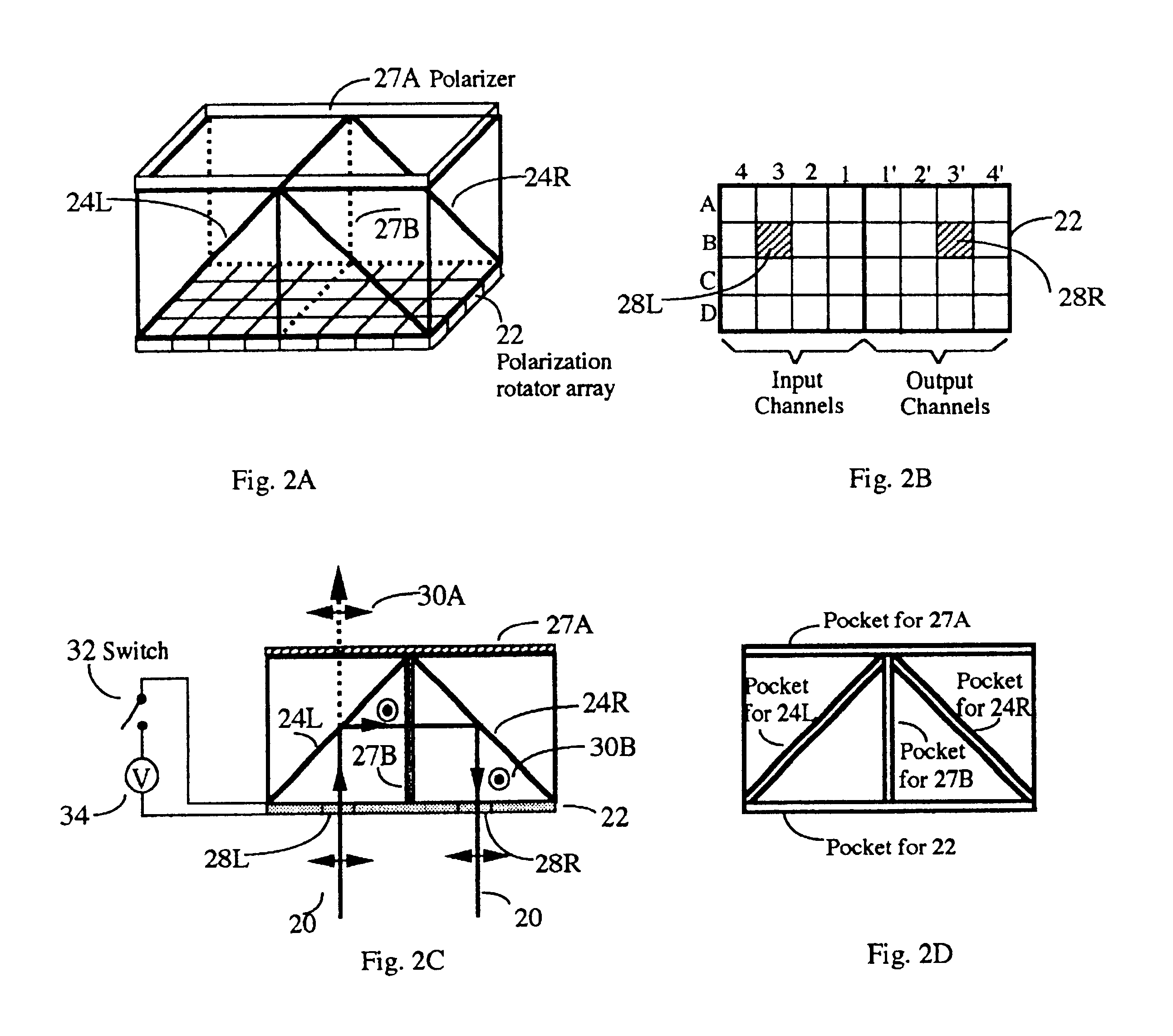
[0041]Referring to FIG. 2A, the basic building block of a ladder-structured variable delay unit of this invention consists of a polarization rotator array 22, two polarization beamsplitters (PBS) 24L and 24R, an optional horizontal polarizer 27A, and an optional vertical polarizer 27B. Polarization rotator array 22 is shown in FIG. 2B and it may comprise of liquid crystal polarization rotators, magneto-optical polarization rotators, or electrooptical polarization rotators. In the array, each pair of rotators 28L and 28R defines a signal channel and can be independently controlled. The pair should always be in the same state. For example, rotators (B,j) and (B,j′) in FIG. 2B should be “on” or “off” simultaneously, where j and j′ are coordinate integers. All channels in the block share the same polarization beamsplitters and polarizers. As shown in FIG. 2C, when a switch 32 and a control signal 34 activate a polarization rotator 28L, a horizontal polarization state 30A of an incoming ...
PUM
 Abstract
Description
Claims
Application Information