
Photonic variable delay devices based on optical birefringence

a technology of birefringence and delay device, which is applied in the direction of instruments, electrical equipment, and antennas, can solve the problems of affecting the accuracy of phased array radar, etc., and achieves low loss, high packing density, and easy fabrication.

Inactive Publication Date: 2005-10-04
GENERAL PHOTONICS CORP
View PDF11 Cites 32 Cited by
  • Summary
  • Abstract
  • Description
  • Claims
  • Application Information

AI Technical Summary

Problems solved by technology

For a phased array of a wide instantaneous bandwidth, adjusting only the relative phase is not sufficient and so a relative time delay adjustment of the radiating elements must be introduced to avoid the beam pointing error known as squint, which results from the modification of the antenna phase pattern with changing frequency.
Conventional electronic beam forming systems for generating and delivering the requisite time delay and phase information are generally bulky, lossy, inefficient, and of narrow bandwidth.
None of the proposed photonic beam forming networks to date meet all of the above requirements.
1824-828, 1990) are limited to below 5 GHz and suffer from poor delay resolution, and therefore not adequate for mm-wave phased arrays.
264-21, 1992) are complicated, and are characterized by high loss, high cost, poor delay resolution, and one-dimensional geometry.
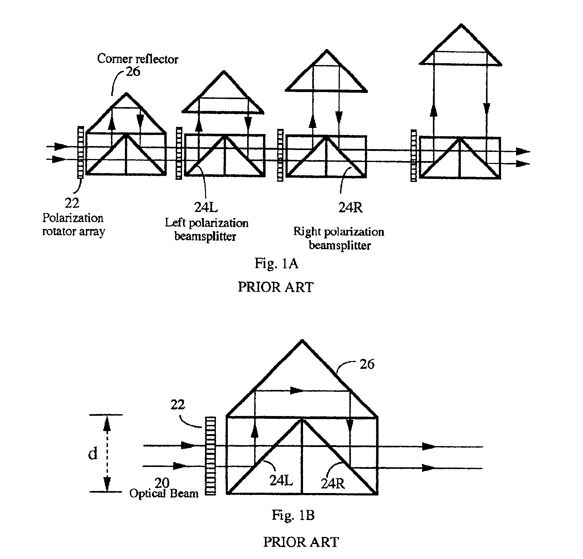
However, as shown in FIG. 1B, the delay resolution of the device is limited by the size of the vertical dimension d of the two dimensional delay array and equals to 2dn, where n is the refractive index of the required polarization beam splitting cube.
In addition, presently the path-switched true time delay has a non-optimized design, making it bulky, expensive, and difficult to manufacture.
Other frequencies will destructively interfere and suffer severe loss—a bandpass filter is formed.
Because such a delay line involves mechanical moving parts, it is generally bulky, heavy, difficult to align, and less reliable.
In addition, because the piezo-electric transducer suffers from hysteresis and temperature dependent drift, active control using feedback servo loop is required, resulting in a complicated system.
The delay resolution of the device is sufficiently fine for accurate beam steering, and the total delay is adequately large to cover desired scanning angles.

Method used


Image

  • Photonic variable delay devices based on optical birefringence
  • Photonic variable delay devices based on optical birefringence
  • Photonic variable delay devices based on optical birefringence

Examples


Embodiment Construction

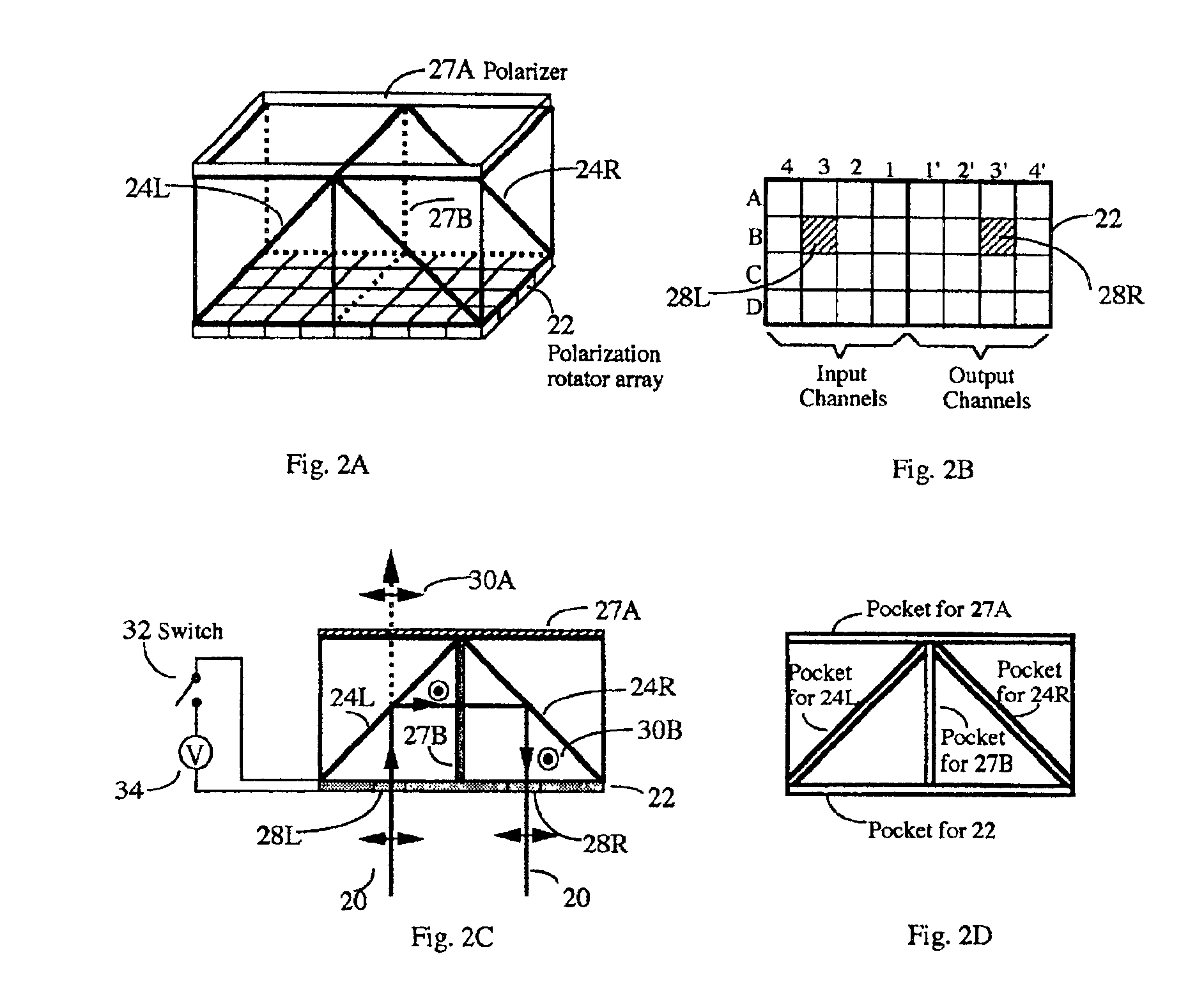
[0041]Referring to FIG. 2A, the basic building block of a ladder-structured variable delay unit of this invention consists of a polarization rotator array 22, two polarization beamsplitters (PBS) 24L and 24R, an optional horizontal polarizer 27A, and an optional vertical polarizer 27B. Polarization rotator array 22 is shown in FIG. 2B and it may comprise of liquid crystal polarization rotators, magnetooptical polarization rotators, or electrooptical polarization rotators. In the array, each pair of rotators 28L and 28R defines a signal channel and can be independently controlled. The pair should always be in the same state. For example, rotation (Bj) and (Bj′) in FIG. 2B should be “on” or “off” simultaneously, where j and j′ are coordinate integers. All channels in the block share the same polarization beamsplitters and polarizers. As shown in FIG. 2C, when a switch 32 and a control signal 34 activate a polarization rotator 28L, a horizontal polarization state 30A of an incoming lig...


PUM

PropertyMeasurementUnit
mm-wave frequenciesaaaaaaaaaa
diameteraaaaaaaaaa
wavelengthaaaaaaaaaa

Abstract

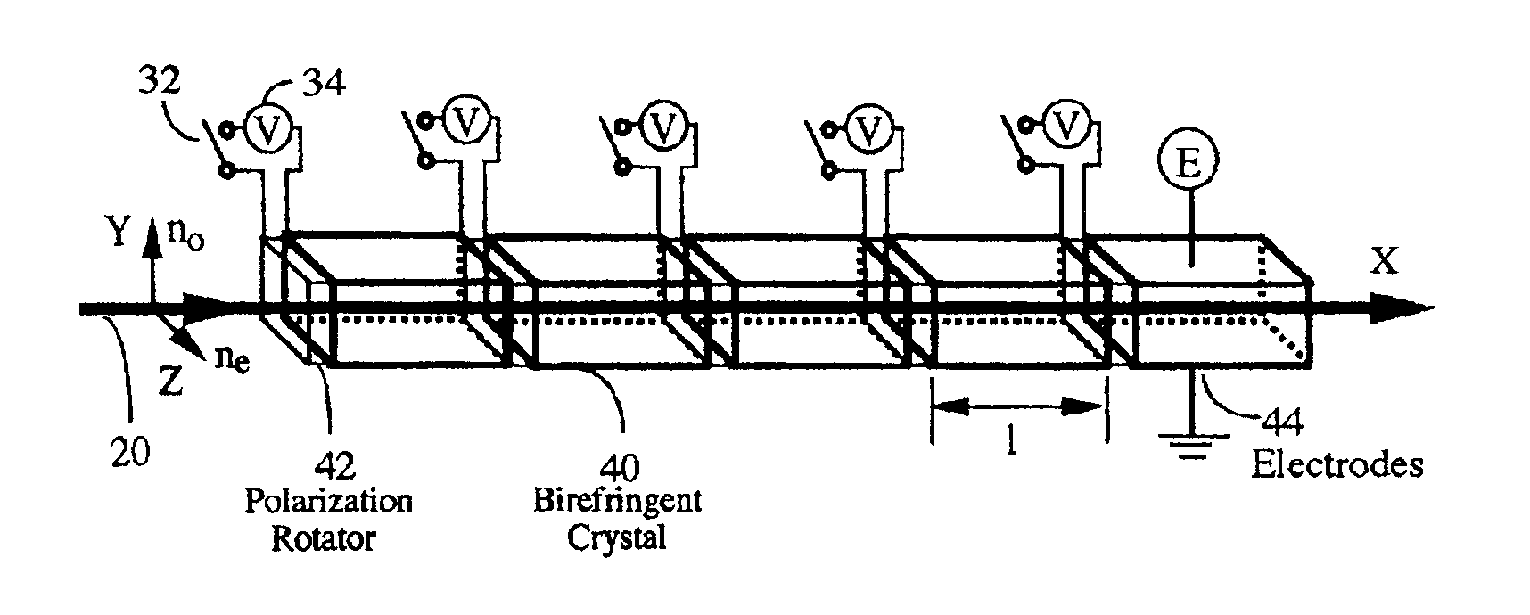
Optical variable delay devices for providing variable true time delay to multiple optical beams simultaneously. A ladder-structured variable delay device comprises multiple basic building blocks stacked on top of each other resembling a ladder. Each basic building block has two polarization beamsplitters and a polarization rotator array arranged to form a trihedron; Controlling an array element of the polarization rotator array causes a beam passing through the array element either going up to a basic building block above it or reflect back towards a block below it. The beams going higher on the “ladder” experience longer optical path delay. An index-switched optical variable delay device comprises of many birefringent crystal segments connected with one another, with a polarization rotator array sandwiched between any two adjacent crystal segments. An array element in the polarization rotator array controls the polarization state of a beam passing through the element, causing the beam experience different refractive indices or path delays in the following crystal segment. By independently control each element in each polarization rotator array, variable optical path delays of each beam can be achieved. Finally, an index-switched variable delay device and a ladder-structured variable device are cascaded to form a new device which combines the advantages of the two individual devices. This programmable optic device has the properties of high packing density, low loss, easy fabrication, and virtually infinite bandwidth. The device is inherently two dimensional and has a packing density exceeding 25 lines / cm2. The delay resolution of the device is on the order of a femtosecond (one micron in space) and the total delay exceeds 10 nanosecond. In addition, the delay is reversible so that the same delay device can be used for both antenna transmitting and receiving.

Description

[0001]This invention was made with Government support under a Contract awarded by NASA, and is subject to the provisions of Public Law 96-517 (35 U.S.C 202) in which the inventor is granted right to retain title. The government has certain rights in this invention.[0002]This is a broadening reissue application of the U.S. Pat. No. 5,978,125 which has been surrendered to the U.S. Patent and Trademark Office. Another broadening reissue application, Ser. No. 10 / 002,947, of the same U.S. Pat. No. 5,978,125 was filed on Oct. 31, 2001.FIELD AND ORIGIN OF INVENTION[0003]This invention pertains generally to the precision optical path length control, specifically to a photonic variable true time delay device for steering phased array radar, for constructing a transversal filter, and for controlling the optical path in optical interferometry.BACKGROUND AND SUMMARY OF THE INVENTION[0004]Phased array antennas have the important ability of beam steering without mechanical actuators. This feature...

Claims


Application Information

Patent Timeline
Patent Type & Authority Patents(United States)
IPC IPC(8): G02F1/01H01Q15/14H01Q15/24H01Q3/26H01Q15/00H01Q15/18G02B6/28G02F1/03G02F1/29
CPCG02B6/2861G02F2201/20H01Q3/2682H01Q15/18H01Q15/246
Inventor YAO, X. STEVE
Owner GENERAL PHOTONICS CORP
Learn More