

2.5-dimensional photon crystal-face transmitting laser
A technology for emitting lasers and crystal surfaces, applied in the field of stimulated emission of optical devices, can solve the problems of increased optical loss, inability to couple, and inability to achieve zero-threshold lasing
- Summary
- Abstract
- Description
- Claims
- Application Information
AI Technical Summary
Problems solved by technology
Method used
Image

Examples
Embodiment
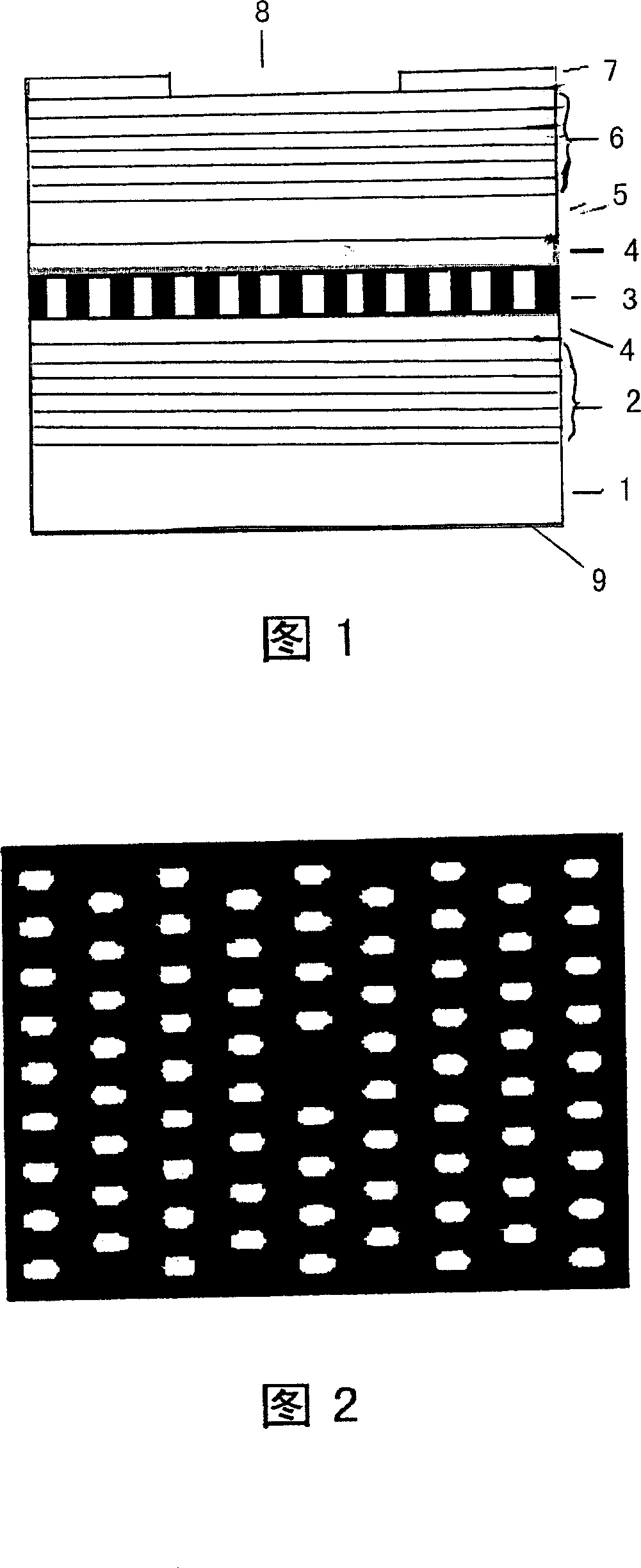
[0034] Please refer to FIG. 1 again. On the n-type GaAs substrate 1, metal oxide chemical vapor deposition (MOCVD) or molecular beam epitaxy (MBE) is used to deposit a multi-layer dielectric high-reflection film with alternating high and low refractive indices, that is, distributed Bragg The reflector (the first DBR layer 2) is used as the lower DBR of the laser. The DBR adopts a quarter-wavelength gallium arsenide (GaAs) and aluminum gallium arsenide (AlGaAs) alternately distributed multilayer thin film structure, in the first DBR layer The lower cladding layer 4 of the laser active region is deposited on the upper cladding layer 2 of the laser, the active layer 3 of the laser is grown on the lower cladding layer 4, and then a planar photonic crystal structure is made on the active layer 3, and the photonic crystal structure contains defects, as shown in Figure 2. The photonic crystal structure can be realized by a variety of common photonic crystal manufacturing methods, suc...
PUM
 Abstract
Description
Claims
Application Information