
CMOSImage sensor and manufacturing method therefor

A technology of image sensor and manufacturing method, which is applied in semiconductor/solid-state device manufacturing, radiation control devices, electrical components, etc., can solve the problems of high dark current and low photosensitivity, and achieve low dark current, high photosensitivity, and good photosensitivity The effect of sensitivity

Inactive Publication Date: 2008-12-10
SEMICON MFG INT (SHANGHAI) CORP +1
View PDF5 Cites 0 Cited by
  • Summary
  • Abstract
  • Description
  • Claims
  • Application Information

AI Technical Summary

Problems solved by technology

[0008] Therefore, the object of the present invention is to provide a CMOS image sensor with low dark current and high photosensitivity to solve the problems of high dark current or low photosensitivity of existing CMOS image sensors

Method used


Image

  • CMOSImage sensor and manufacturing method therefor
  • CMOSImage sensor and manufacturing method therefor
  • CMOSImage sensor and manufacturing method therefor

Examples


Embodiment Construction

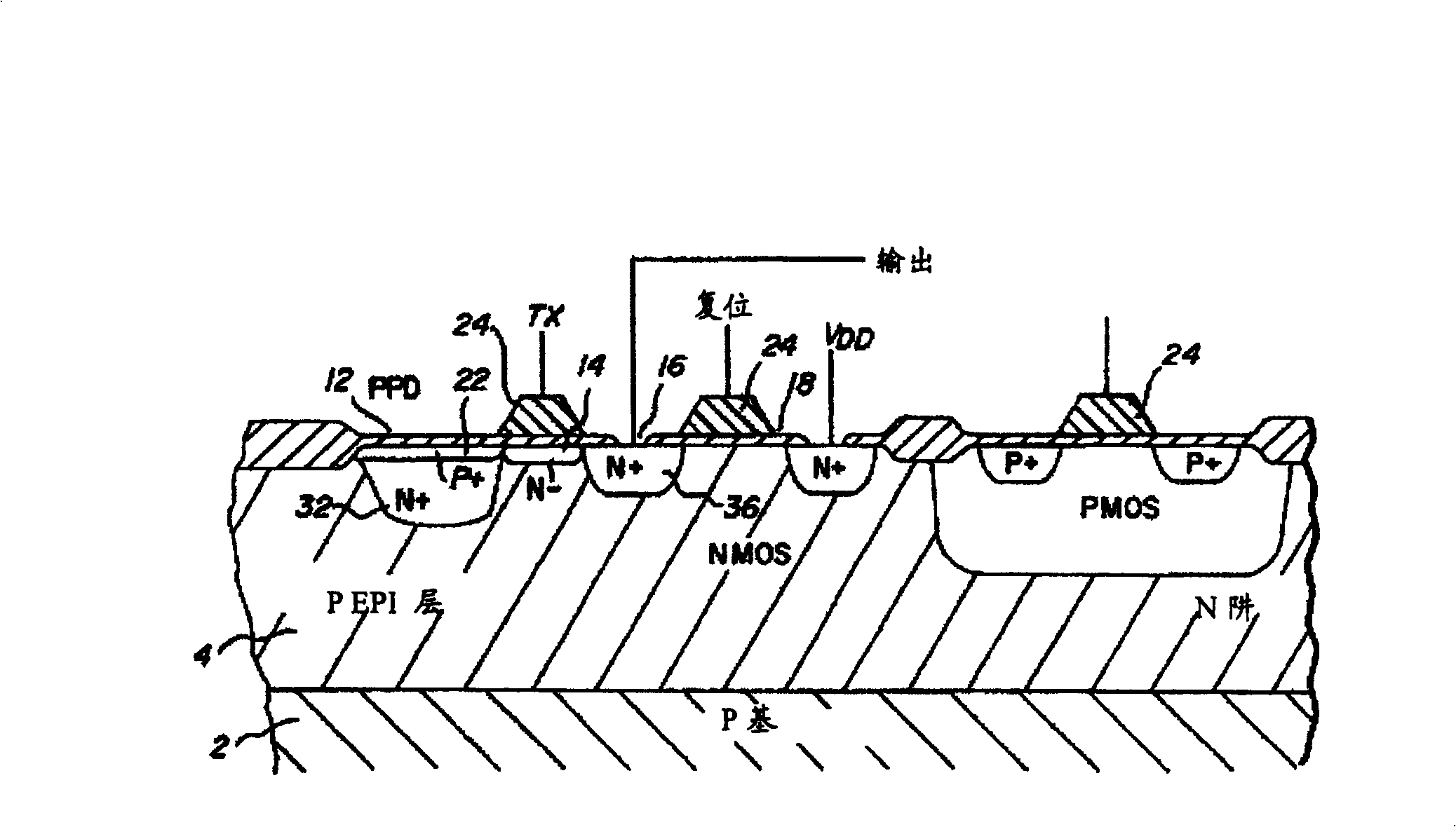
[0047] The CMOS image sensor of the present invention includes a photodiode area and a logic area. The logic area includes a source follower and a row gate. The photodiode region adopts a non-standard manufacturing method, and includes a field oxide region and an active region, on which a reset transistor and a photodiode are formed. The photodiode has a first pole and a second pole, wherein the first pole has a buried region surrounding the bottom and sidewalls of the field oxide region, and a needle-shaped region extending to the upper end of the buried region toward the reset transistor. The buried region isolates the junction of the photodiode from the bottom and edges of the field oxide region, thereby eliminating dark current that may exist at the bottom and edges of the field oxide region. The needle-shaped region is extremely sensitive to light because it is not covered by the field oxide region.

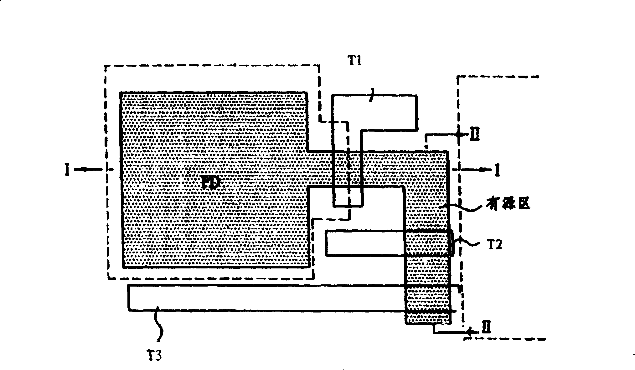
[0048] image 3 Shown is a layout diagram of unit pixels in the CMOS...


PUM


Abstract

A CMOS image sensor includes photodiode area and logic area, the photodiode area includes restoration transistor and photodiode, the photodiode possesses the first pole and the second pole, the first pole possesses bury area which is at the below and side wall of the circling field oxidation area, and pin area which extends towards the direction of the restoration transistor which is above the bury area. Correspondingly, the manufacturing method of the CMOS image sensor includes: forming limiting field and groove of source area; forming adulteration area; injecting the first impurity ion to the lower of the groove and adulteration area to form the bury area and pin area of the first pole of the photodiode; injecting the silicon oxide to the groove to form field oxidation area; the second impurity ion is injected to the upper of the first pole to form the second pole of the photodiode. The bury area of the invention separates the node of the photodiode from the bottom and edge of the filed oxidation area, so the dark current of the bottom and edge of the filed oxidation area is eliminated, because the pin area is not covered by the field oxidation area, so it is very sensitive to light.

Description

technical field [0001] The invention relates to a CMOS image sensing device, in particular to a CMOS image sensing device and a manufacturing method thereof. Background technique [0002] CMOS image sensors have become the dominant solid-state imaging technology primarily due to their lower cost relative to charge-coupled device (CCD) imaging devices. In addition, for some applications, CMOS devices offer superior performance. The pixel element in the CMOS device can be made relatively small, so it can provide a higher division rate than the CCD image sensor. In addition, the signal processing logic can be integrated side-by-side with the imaging circuit, so that a complete stand-alone imaging device can be formed from a single integrated chip. [0003] A CMOS image sensor refers to an image sensor that has active devices such as transistors within each pixel. Conventional CMOS image sensors typically employ photodiodes as the image sensing elements. The most common activ...

Claims


Application Information

Patent Timeline
Patent Type & Authority Patents(China)
IPC IPC(8): H01L27/146H01L21/8234
Inventor 杨建平霍介光辛春艳蔡巧明吴永皓
Owner SEMICON MFG INT (SHANGHAI) CORP
Learn More