Memory cell

A technology for accessing memory and transistor units, which is applied in the field of non-volatile memory units, can solve problems such as increasing the density of storage devices, and achieve the effect of high storage capacity

Inactive Publication Date: 2009-01-14
QS SEMICON AUSTRALIA
View PDF12 Cites 0 Cited by
  • Summary
  • Abstract
  • Description
  • Claims
  • Application Information

AI Technical Summary

Problems solved by technology

This will undoubtedly increase the density of memory devices

Method used


Image

  • Memory cell
  • Memory cell
  • Memory cell

Examples


Embodiment Construction

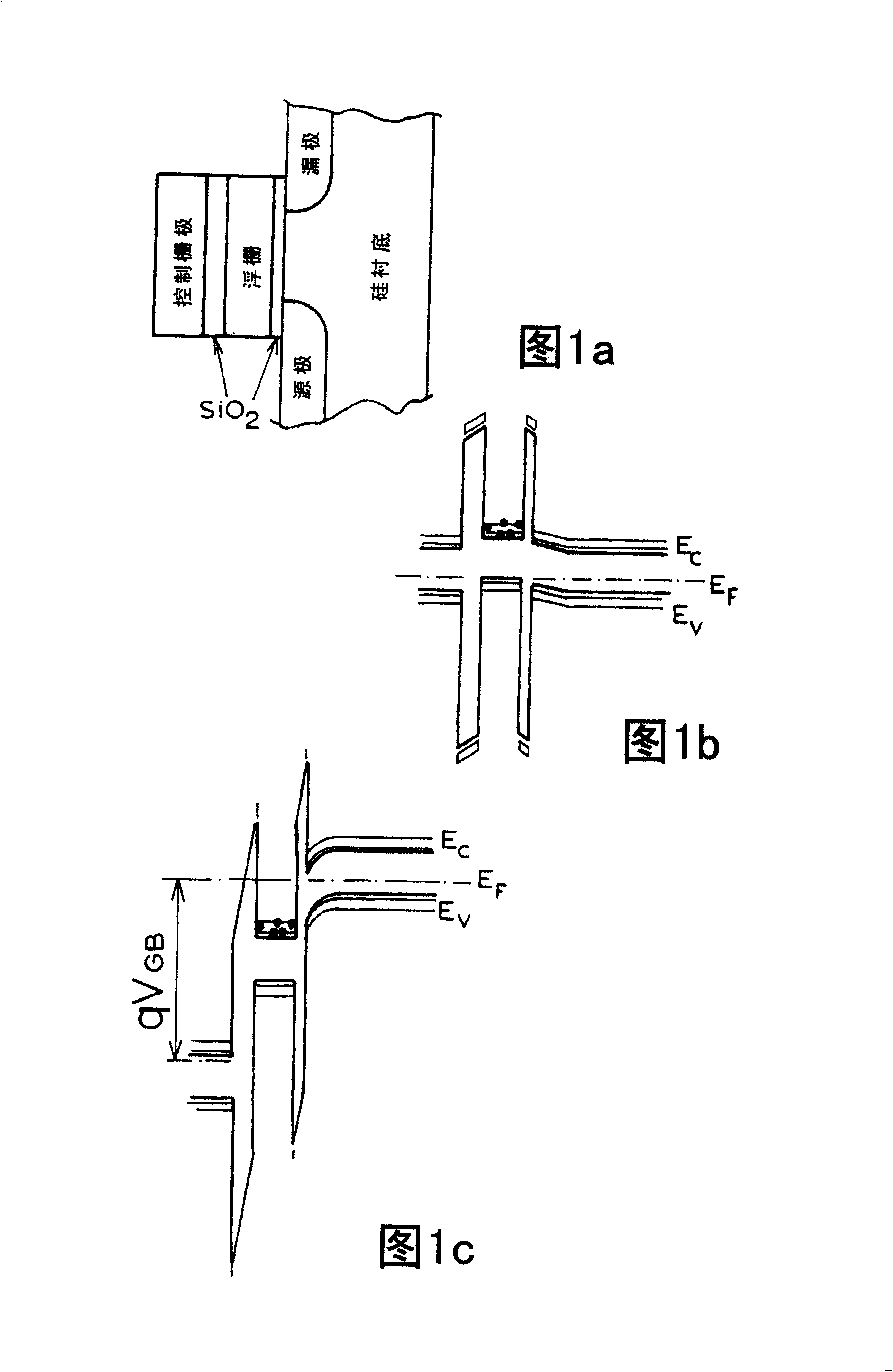
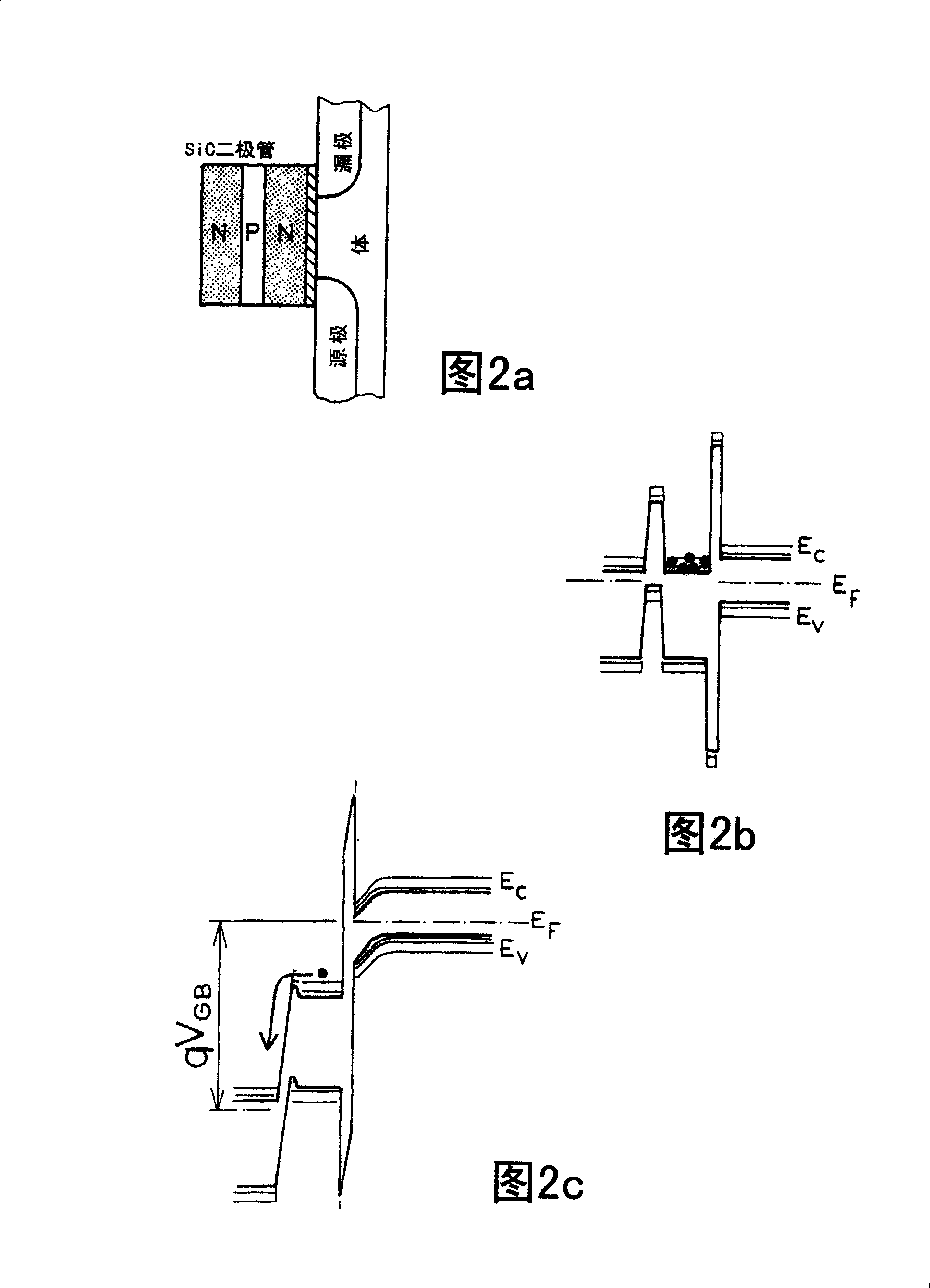
[0068] 1T unit with diode isolation

[0069] Such units are preferred embodiments of the invention. The difference to the capacitor isolation 1T cell used in modern flash memory can be stated simply as follows: The capacitor between the floating gate and the control gate is replaced with a SiC diode.

[0070] Figure 1 shows the cross section and energy band diagram of a capacitor isolated 1T cell. The case of zero voltage between the control gate and the body of the MOSFET (Fig. 1b) shows that electrons are trapped in the potential well created by the floating gate and the surrounding gate dielectric. This allows long charge retention times, since even unbalanced charges cannot escape the high potential barrier created by the capacitor dielectric on both sides. The case of a positive voltage applied to the control gate (Fig. 1c) shows no change in the barrier height between the floating gate and the dielectric of either capacitor. This causes problems in terms of charge r...


PUM


Abstract

A one-transistor (1T) NVRAM cell utilizing silicon carbide (SiC) to provide unbalanced charge isolation and fast and non-destructive charge / discharge. To be able to sense controlled resistances (and many memory levels) instead of capacitors, the cells incorporate memory transistors that can be implemented in silicon or SiC. The 1T cell has diode isolation to enable structures used in current flash memories, especially NOR and NAND arrays. 1T cells with diode isolation are not limited to SiC diodes. The fabrication method includes the formation of a nitrided silicon dioxide gate on a SiC substrate, followed by ion implantation, followed by the steps of self-aligned MOSFET formation.

Description

technical field [0001] The present invention relates to non-volatile memory cells, and more particularly to silicon carbide-based memory cells. Background technique [0002] DRAM devices in current silicon-based technologies are volatile because the stored information must be refreshed periodically and is lost when the memory cell is no longer connected to a power source. [0003] Flash memory provides complementary functions in modern electronic systems. Flash memory uses floating gates, which are charged or discharged through surrounding insulating material to change logic states. It is read-only memory (ROM) and cannot be used for RAM applications because it takes too long to write information and is limited to a certain number of write cycles. However, it provides non-volatile storage of information that is retained even if power is disconnected from the storage unit. Flash memory is also process dependent, and actually needs to be tuned for process by compensating fo...

Claims


Application Information

Patent Timeline
Patent Type & Authority Patents(China)
IPC IPC(8): G11C11/36G11C11/40G11C11/401G11C11/41
Inventor 巴里·H·哈里森西马·迪米特里耶夫
Owner QS SEMICON AUSTRALIA
Why Eureka
Try Eureka