Packing structure of chip inverted-mounted light-emitting diode and packing method thereof

A light-emitting diode and flip-chip technology, applied in electrical components, electric solid-state devices, circuits, etc., can solve the problems of LED degradation, small contact area, reduced luminous efficiency, etc. Effect

Active Publication Date: 2009-02-11
EPISTAR CORP
View PDF3 Cites 0 Cited by
  • Summary
  • Abstract
  • Description
  • Claims
  • Application Information

AI Technical Summary

Problems solved by technology

Although this packaging method can improve the above-mentioned shortcoming of reduced luminous efficiency caused by light shielding, the heat generated by the LED 10 can only be conducted to the printed circuit board 40 through the metal bump 43. On the one hand, the contact area for conduction is small, and on the other hand On the one hand, the thermal conductivity of the printed circuit board 40 is limited, and the overall heat dissipation efficiency of the LED 10 cannot be effectively improved, so there are still the aforementioned disadvantages of LED deterioration and luminosity reduction due to high temperature

Method used


Image

  • Packing structure of chip inverted-mounted light-emitting diode and packing method thereof
  • Packing structure of chip inverted-mounted light-emitting diode and packing method thereof
  • Packing structure of chip inverted-mounted light-emitting diode and packing method thereof

Examples


Embodiment Construction

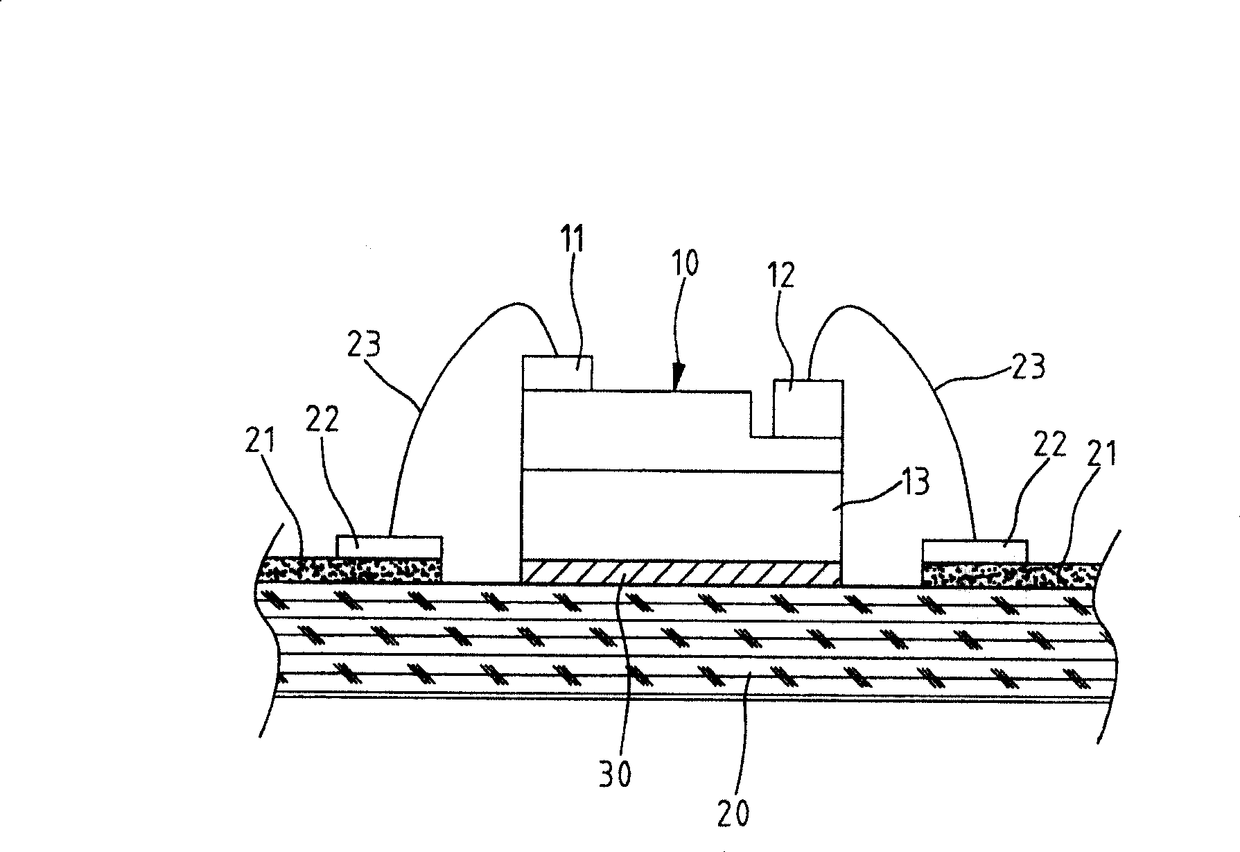
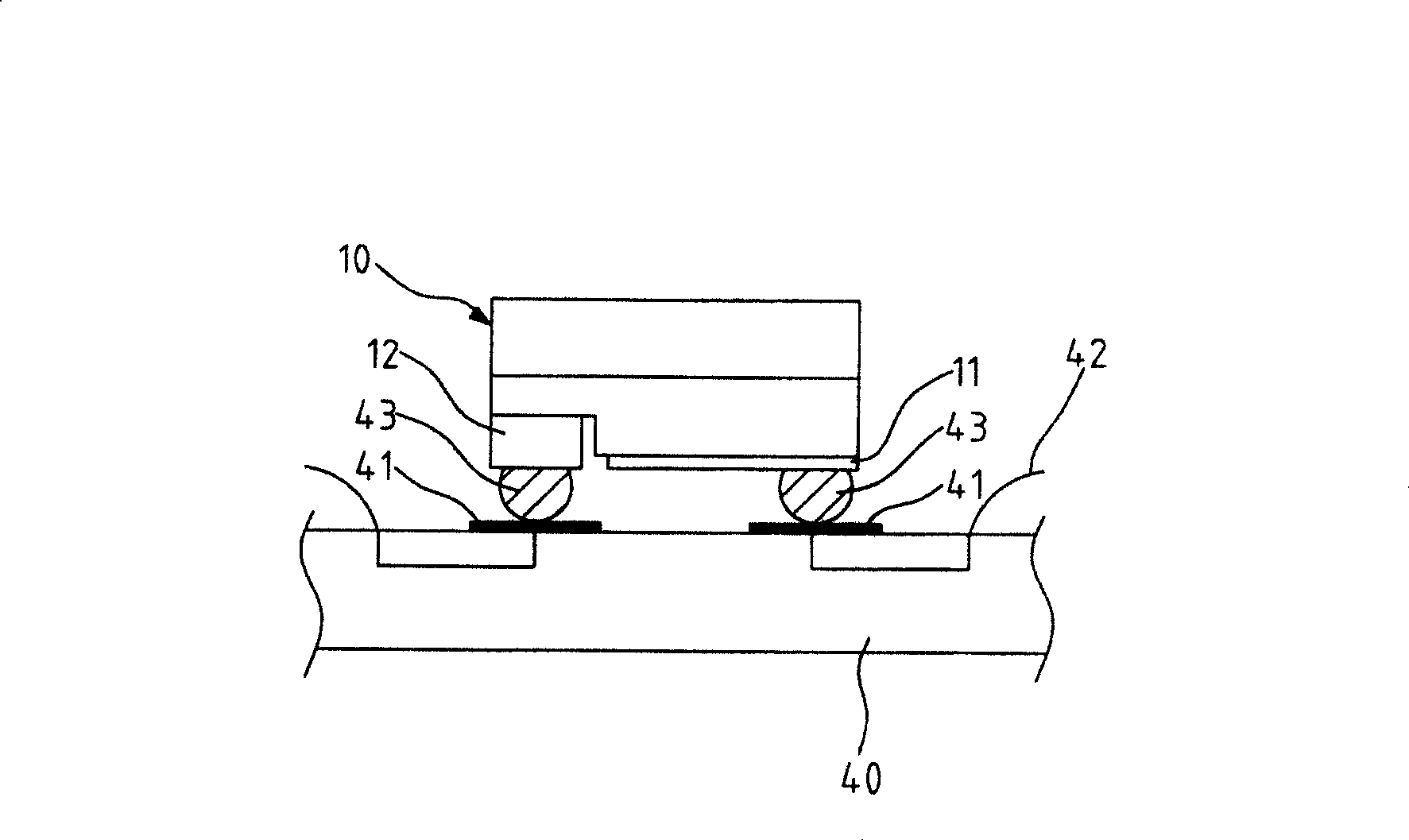
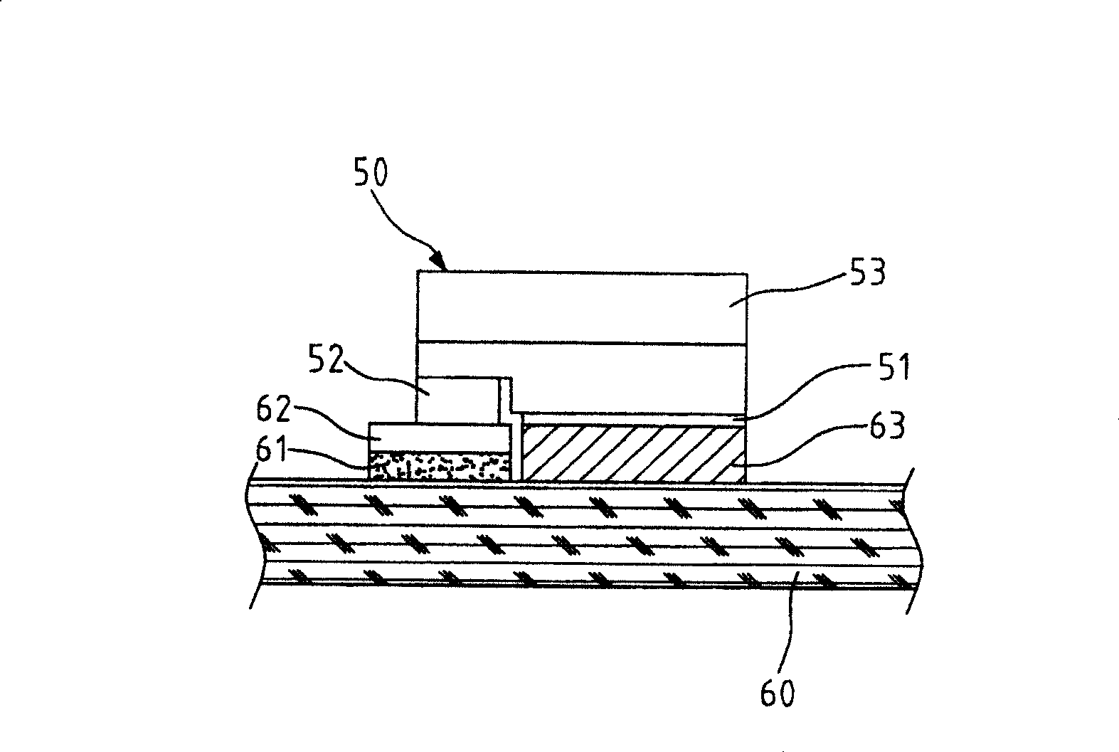
[0014] see image 3 , which is a schematic diagram of an embodiment of the present invention. The packaging structure of the flip-chip light emitting diode of the present invention includes an LED 50 and a heat-conducting substrate 60 , and the LED 50 is packaged on the heat-conducting substrate 60 in a flip-chip manner.

[0015] The LED 50 includes a first electrode 51 and a second electrode 52 , the first electrode 51 and the second electrode 52 are located on the same side of the surface of the LED 50 . The electrodes can be made by plating titanium (Ti), aluminum or gold (Au) and other metal layers by physical vapor deposition (Physical Vapor Deposition, PVD), and then through metal fusion. On a general gallium nitride (GaN) LED chip, the first electrode 51 can be electrically connected to the P-type gallium nitride (P-GaN) layer to become a P-type electrode, while the second electrode 52 can be connected to the N-type nitrogen The gallium nitride (n+GaN) layers are elec...


PUM


Abstract

The invention is concerned with the covering crystal LED sealing structure and the sealing method that is with high radiating efficiency. The structure is: seals the LED on the radiating plaque by the covering crystal technique assorting sharing crystal linking mode. The structure consists of: the radiating plaque that forms the insolating layer in the prearrange area and the surface of the insolating layer forms the welding underlay; the LED that links on the radiating plaque by the covering mode, the LED consists of the first electrode and the second electrode, the first electrode and the radiating plaque sharing crystal link with the sharing layer in order to electric connect, the second electrode electric connects with the welding underlay.

Description

technical field [0001] The present invention relates to a packaging structure of a light emitting diode (Light Emitting Diode, LED), in particular to a flip-chip LED packaging structure with high heat dissipation efficiency and a packaging method thereof. Background technique [0002] Due to the characteristics of small size, low power consumption, and long service life, LED light sources will replace current lighting equipment such as light bulbs or fluorescent light sources or light sources of other display devices in the foreseeable future, and become the most important light-emitting components. . However, in order to increase the overall brightness of the light source, it is necessary to increase the luminous power or increase the number or density of LED installations, but such settings will greatly increase the heat generated by the LED light source. If the heat cannot be exported as soon as possible, it will seriously affect the performance of the LED. Luminous brig...

Claims


Application Information

Patent Timeline
Patent Type & Authority Patents(China)
IPC IPC(8): H01L33/00H01L23/36H01L23/488H01L21/60H01L33/48H01L33/62H01L33/64
CPCH01L2224/49107H01L24/14H01L2224/48091H01L2224/16225H01L2224/73265H01L2224/48227H01L2224/32225H01L2224/14H01L2924/01322H01L2924/12041H01L2924/00014H01L2924/00H01L2924/00012
Inventor 董经文
Owner EPISTAR CORP
Why Eureka
Try Eureka