Microelectronic element with elastic conductive projection and method of manufacture

A microelectronic component, elastic conductive technology, applied in the field of microelectronics, can solve the problems of increased connection resistance, short circuit, open circuit, etc., and achieve the effect of avoiding excessive connection resistance or even open circuit

Inactive Publication Date: 2009-07-08
SHANGHAI JIAOTONG UNIV
View PDF3 Cites 0 Cited by
  • Summary
  • Abstract
  • Description
  • Claims
  • Application Information

AI Technical Summary

Problems solved by technology

A problem brought about by this is that the number of conductive particles between the conductive bump and the connection terminal becomes too small due to the escape of conductive particles during the packaging process, which increases the connection resistance and even causes an open circuit
Another problem brought about by this is: too many conductive particles are concentrated between adjacent conductive bumps, forming a lateral electrical connection, that is, causing a short circuit to adjacent conductive bumps and adjacent connection terminals

Method used


Image

  • Microelectronic element with elastic conductive projection and method of manufacture
  • Microelectronic element with elastic conductive projection and method of manufacture
  • Microelectronic element with elastic conductive projection and method of manufacture

Examples


Embodiment Construction

[0036] The present invention will be described more fully hereinafter with reference to the accompanying drawings, in which preferred embodiments of the invention are shown.

[0037] The embodiments will be described with reference to a liquid crystal display driver chip (hereinafter simply referred to as a driver chip) as a microelectronic element, the characteristics of which will be described by way of example.

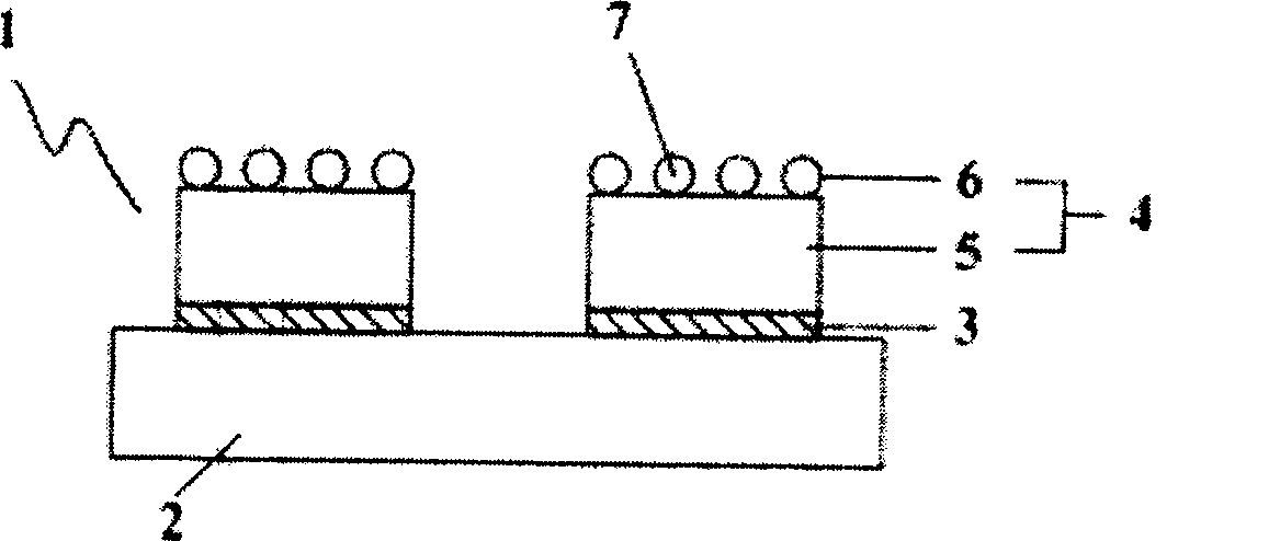
[0038] figure 1 It is a structural schematic diagram of a driving chip with elastic conductive bumps according to an embodiment of the present invention.

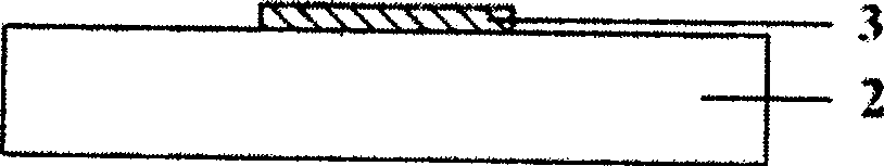
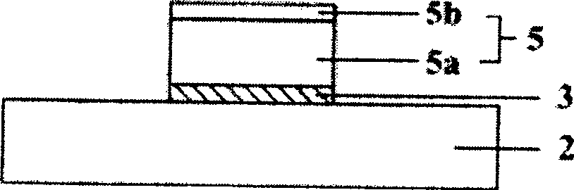
[0039] In view of the previous description of the problems faced by the current packaging structure using ACF for flip-chip interconnection, an embodiment of the present invention provides a driving chip 1 with elastic conductive bumps 4, including a semiconductor chip 2 and a The elastic conductive bump 4 on the bonding pad 3 on the surface of the semiconductor chip. It is characterized in that the elastic co...


PUM

PropertyMeasurementUnit
thicknessaaaaaaaaaa
diameteraaaaaaaaaa

Abstract

The present invention provides a microelectronic element (1) and method of manufacturing the same. The microelectronic element (1) comprises a semiconductor chip (2) and a bump (4) located on the pad (3) of the semiconductor chip (2). The bump (4) includes a conductive layer (5) and an elastic conductor layer (6). The conductive layer (5) is connected with the pad (3) of the semiconductor chip (2) and the elastic conductor layer (6) is fixed on the conductive layer (5) by inter-metallic connection. The elastic conductor layer (6) consists of conductive particles (7). The present invention also provides a package structure and a LCD device (15) including the microelectronic element (1). There is no need for anisotropic conductive film in method of manufacturing the microelectronic element (1).

Description

technical field [0001] The invention relates to the technical field of microelectronics, and specifically provides a microelectronic element with elastic conductive bumps, including a packaging structure of the microelectronic element, a liquid crystal display device, and a manufacturing method of the microelectronic element. Background technique [0002] In the existing microelectronics manufacturing technology field, flip chip (Flip Chip, FC) technology using anisotropic conductive film (Anisotropic Conductive Film, ACF) as the interconnection medium plays a very important role. Take the currently commonly used ACF as an example. It is composed of a high molecular polymer and conductive particles uniformly dispersed in it. The diameter of the conductive particles is about 3 to 5 microns. It is usually a resin particle with a conductive metal material on the surface. . [0003] Among the existing flip-chip technologies, the widely used manufacturing process of ACF mainly i...

Claims


Application Information

Patent Timeline
Patent Type & Authority Patents(China)
IPC IPC(8): H01L23/485H01L23/488H01L21/60G02F1/133
CPCH01L2924/01049H01L2924/09701H01L2924/01051H01L2924/07802H05K3/305H01L2224/81801H01L24/12H05K2201/0233H01L2924/01015H01L2924/0105H01L2924/1461H05K3/102H01L2924/01327H01L2924/00013H01L2924/01047H01L2224/1147H01L2924/01046H01L2924/01078H01L2924/01006H05K2201/10977H05K3/325H01L24/11H01L2924/01079H01L2924/01074H01L2924/14G02F1/13452H01L2224/16H01L2924/01024H01L2924/01005H01L2924/0103H01L2924/01082H01L2924/01013H01L2924/01322H01L2924/01022H01L2924/01029H01L2924/01033H01L24/81H01L24/03H01L24/05H01L24/13H01L2224/0554H01L2224/05568H01L2224/05573H01L2924/00014H01L2224/13099H01L2924/00H01L2224/05599H01L2224/0555H01L2224/0556
Inventor 贾磊王志平丁汉
Owner SHANGHAI JIAOTONG UNIV
Why Eureka
Try Eureka