Extension developing method for high-power semiconductor quanta point laser material
A technology of quantum dots and quantum dot materials, applied in the field of semiconductor lasers, can solve the problems of quantum dot disorder, distribution uniformity and difficult density control
- Summary
- Abstract
- Description
- Claims
- Application Information
AI Technical Summary
Problems solved by technology
Method used
Image
Examples
Embodiment Construction
[0052] The present invention will be described in further detail below in conjunction with accompanying drawing
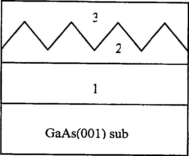
[0053] figure 1 It is the core idea of the present invention, that is, the formation process of epitaxial growth of high-density quantum dots.
[0054] Firstly, a GaAs transition layer 1 is formed on a GaAs(001) substrate with a thickness of 300-500nm and a growth temperature of 600-610°C, and then pause for 20-40 seconds while lowering the temperature to 480-520°C;
[0055] Secondly, the InGaAs quantum dot structure 2 is grown on the GaAs transition layer 1 with a thickness of 5-8ML. The layer point is grown according to the following steps: first, deposit an InAs material layer with a thickness of 0.7-1.4ML, a growth rate of 0.2-0.5ML / s, a temperature of 480-510°C, and a pause of 1-10 seconds, and then deposit a GaAs layer , the thickness is 0.7-1.4ML, the growth rate is 0.2-0.5ML / s, the temperature is 480-510°C, and the pause is 1-10 seconds; repeat the abo...
PUM
 Abstract
Description
Claims
Application Information


