InGaAs/GaAs quantum dot epitaxial structure in wave band between 1.02 to 1.08 micrometer and manufacturing method thereof

A technology of quantum dots and quantum dot materials, applied in the field of semiconductor lasers, can solve the problems of disorder, uniformity of distribution and difficult control of density of quantum dots

Inactive Publication Date: 2010-12-08
INST OF SEMICONDUCTORS - CHINESE ACAD OF SCI
View PDF1 Cites 0 Cited by
  • Summary
  • Abstract
  • Description
  • Claims
  • Application Information

AI Technical Summary

Problems solved by technology

The difficulty of this method is that the nucleation of quantum dots on the wetting layer is disordered, and its shape, size, distribution uniformity and density are not easy to control

Method used


Image

  • InGaAs/GaAs quantum dot epitaxial structure in wave band between 1.02 to 1.08 micrometer and manufacturing method thereof
  • InGaAs/GaAs quantum dot epitaxial structure in wave band between 1.02 to 1.08 micrometer and manufacturing method thereof
  • InGaAs/GaAs quantum dot epitaxial structure in wave band between 1.02 to 1.08 micrometer and manufacturing method thereof

Examples


Embodiment Construction

[0054] The present invention will be described in further detail below in conjunction with accompanying drawing
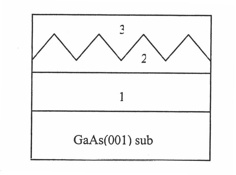
[0055] figure 1 It is the core idea of ​​the present invention, that is, the formation process of epitaxial growth of high-density quantum dots.

[0056] Firstly, a GaAs transition layer 1 is formed on a GaAs(001) substrate with a thickness of 300-500nm and a growth temperature of 600-610°C, and then pause for 20-40 seconds while lowering the temperature to 480-520°C;

[0057] Secondly, the InGaAs quantum dot structure 2 is grown on the GaAs transition layer 1 with a thickness of 5-8ML. The layer point is grown according to the following steps: first, deposit an InAs material layer with a thickness of 0.7-1.4ML, a growth rate of 0.2-0.5ML / s, a temperature of 480-510°C, and a pause of 1-10 seconds, and then deposit a GaAs layer , the thickness is 0.7-1.4ML, the growth rate is 0.2-0.5ML / s, the temperature is 480-510°C, and the pause is 1-10 seconds; repeat the abo...


PUM


Abstract

The invention relates to the technical field of semiconductor lasers, provides an InGaAs / GaAs quantum dot epitaxial structure with 1.02 to 1.08 micron wave band, and an epitaxial growing method for a molecular beam high-power semiconductor quantum dot laser material for realizing the epitaxial structure. The a PL spectrum with 1.02 to 1.08 micron wave band at room temperature can illuminate by precisely controlling the molecular beam epitaxial growing condition, namely using the alternative growth of a monoatomic layer to control components, epitaxial layer thickness, appearance structure andthe like of the quantum dot and has high luminous efficiency. The method is applied to a pumping source of an optical fiber laser, greatly reduces the device volume and the manufacturing cost and keeps good performance index of the quantum dot laser, such as reducing the threshold current of the laser, reducing the power consumption, improving the temperature stability and the like.

Description

[0001] This case is a divisional application of the previous application number: 2005100863149; invention name: "1.02-1.08 micron band InGaAs / GaAs quantum dot epitaxy structure and its manufacturing method" [0002] 1.02-1.08 micron band InGaAs / GaAs quantum dot epitaxy structure and manufacturing method thereof technical field [0003] The invention relates to the technical field of semiconductor lasers, in particular to a 1.02-1.08 micron band InGaAs / GaAs quantum dot epitaxy structure and a manufacturing method thereof. Background technique [0004] An important application of semiconductor lasers in the 1.02-1.08 micron band can be used to pump fiber lasers. Because fiber laser has the characteristics of high gain, high slope efficiency, narrow line width, broadband tunable, good heat dissipation, compact structure, miniaturization, full curing and natural compatibility with transmission fiber, it is widely used in communication, military, medical and optical Information ...

Claims


Application Information

Patent Timeline
Patent Type & Authority Patents(China)
IPC IPC(8): H01S5/30
Inventor 于理科徐波王占国金鹏赵昶张秀兰
Owner INST OF SEMICONDUCTORS - CHINESE ACAD OF SCI
Why Eureka
Try Eureka