Extension developing method for high-power semiconductor quanta point laser material

A technology of quantum dot materials and growth methods, which is applied in the field of epitaxial growth of high-power semiconductor quantum dot laser materials, and can solve problems such as distribution uniformity and density, difficulty in controlling quantum dots, and disordered quantum dots

Inactive Publication Date: 2007-03-07
INST OF SEMICONDUCTORS - CHINESE ACAD OF SCI
View PDF0 Cites 6 Cited by
  • Summary
  • Abstract
  • Description
  • Claims
  • Application Information

AI Technical Summary

Problems solved by technology

The difficulty of this method is that the nucleation of quantum dots on the wetting layer is disordered, and its shape, size, distribution uniformity and density are not easy to control

Method used


Image

  • Extension developing method for high-power semiconductor quanta point laser material
  • Extension developing method for high-power semiconductor quanta point laser material
  • Extension developing method for high-power semiconductor quanta point laser material

Examples


Embodiment Construction

[0057] The present invention will be described in further detail below in conjunction with accompanying drawing
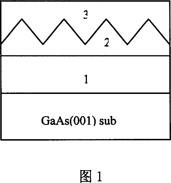
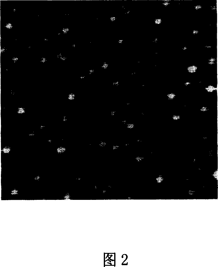
[0058] Fig. 1 is the core idea of ​​the present invention, that is, the formation process of epitaxial growth of high-density quantum dots.

[0059] Firstly, a GaAs transition layer 1 is formed on a GaAs(001) substrate with a thickness of 300-500nm and a growth temperature of 600-610°C, and then pause for 20-40 seconds while lowering the temperature to 480-520°C;

[0060] Secondly, the InGaAs quantum dot structure 2 is grown on the GaAs transition layer 1 with a thickness of 5-8ML. The layer point is grown according to the following steps: first, deposit an InAs material layer with a thickness of 0.7-1.4ML, a growth rate of 0.2-0.5ML / s, a temperature of 480-510°C, and a pause of 1-10 seconds, and then deposit a GaAs layer , the thickness is 0.7-1.4ML, the growth rate is 0.2-0.5ML / s, the temperature is 480-510°C, and the pause is 1-10 seconds; repeat the above proc...


PUM


Abstract

This invention relates to semiconductor laser technique field and provides one InGaAs / GaAs SK growth high intensity quantum point extension layer structure to realize this extension molecule beam semiconductor quantum laser materials method. Through accurate control molecule beam extension growing condition and using submolecule single layer to control quantum points component, extensive thickness, shape structure to realize room temperature PL spectrum of 1.02-1.08 micrometer band.

Description

technical field [0001] The invention relates to the technical field of semiconductor lasers, in particular to an epitaxial growth method for high-power semiconductor quantum dot laser materials. Background technique [0002] An important application of semiconductor lasers in the 1.02-1.08 micron band can be used to pump fiber lasers. Because fiber laser has the characteristics of high gain, high slope efficiency, narrow line width, broadband tunable, good heat dissipation, compact structure, miniaturization, full curing and natural compatibility with transmission fiber, it is widely used in communication, military, medical and optical Information processing and other fields will have broad application prospects, especially in the field of optical communication. With the development of optical wavelength division and optical time division multiplexing technology, fiber lasers will be able to meet the higher requirements of communication systems for light sources It is consi...

Claims


Application Information

Patent Timeline
Patent Type & Authority Applications(China)
IPC IPC(8): H01L33/00H01S5/343
Inventor 于理科徐波王占国金鹏赵昶张秀兰
Owner INST OF SEMICONDUCTORS - CHINESE ACAD OF SCI
Why Eureka
Try Eureka