Method of fabrication SiGe heterojuction bipolar transistor

A device manufacturing method and transistor technology, applied in semiconductor/solid-state device manufacturing, semiconductor devices, electrical components, etc., can solve the problems of low parasitic capacitance and small transistor size, and achieve the effect of simple isolation

Inactive Publication Date: 2009-07-29
NXP BV
View PDF2 Cites 4 Cited by
  • Summary
  • Abstract
  • Description
  • Claims
  • Application Information

AI Technical Summary

Problems solved by technology

[0006] While the gist of US-A-6169007 exhibits the aforementioned advantages of smaller transistor sizes and lower parasitic capacitances, it also exhibits the disadvantages associated with the disclosed fabrication techniques,

Method used


Image

  • Method of fabrication SiGe heterojuction bipolar transistor
  • Method of fabrication SiGe heterojuction bipolar transistor
  • Method of fabrication SiGe heterojuction bipolar transistor

Examples


Embodiment Construction

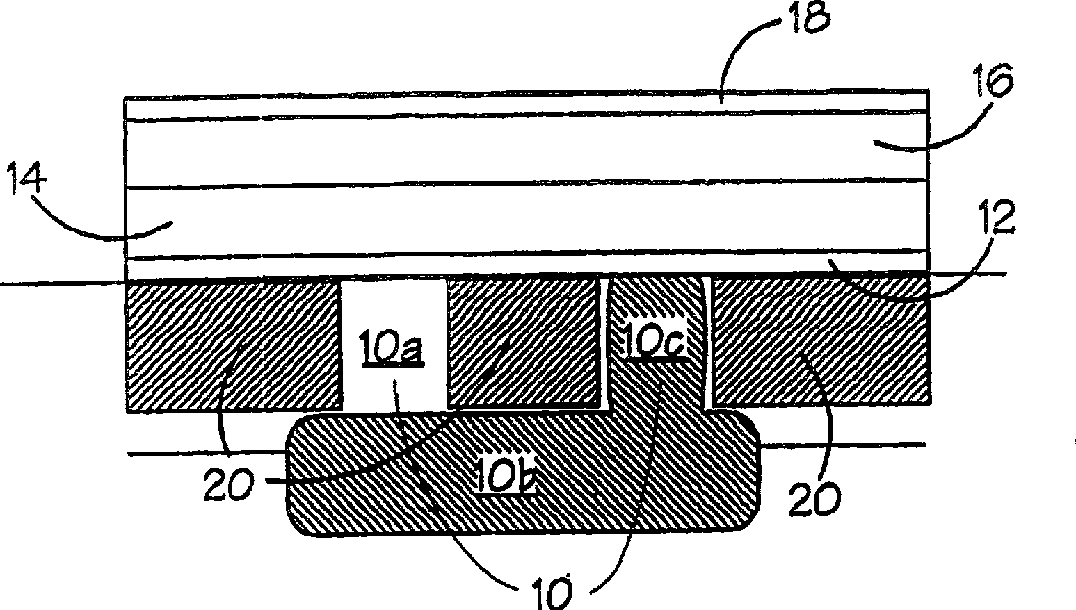
[0021] figure 1 The initial structure is shown, which comprises a standard BiCMOS p-doped substrate 10, represented by a buried collector contact 10b, an N-type collector epitaxial layer 10a, and a surface to provide a buried n-layer collector contact. The contacts between 10b and n plug the dimples 10c. Finally field isolation regions are provided in the form of two shallow trench isolation regions 20 . A thermal oxide layer 12 is grown on top of the substrate 10, followed by a layer stack consisting of a boron in situ doped polysilicon deposition layer 14, a TEOS layer 16, and an amorphous silicon layer 18.

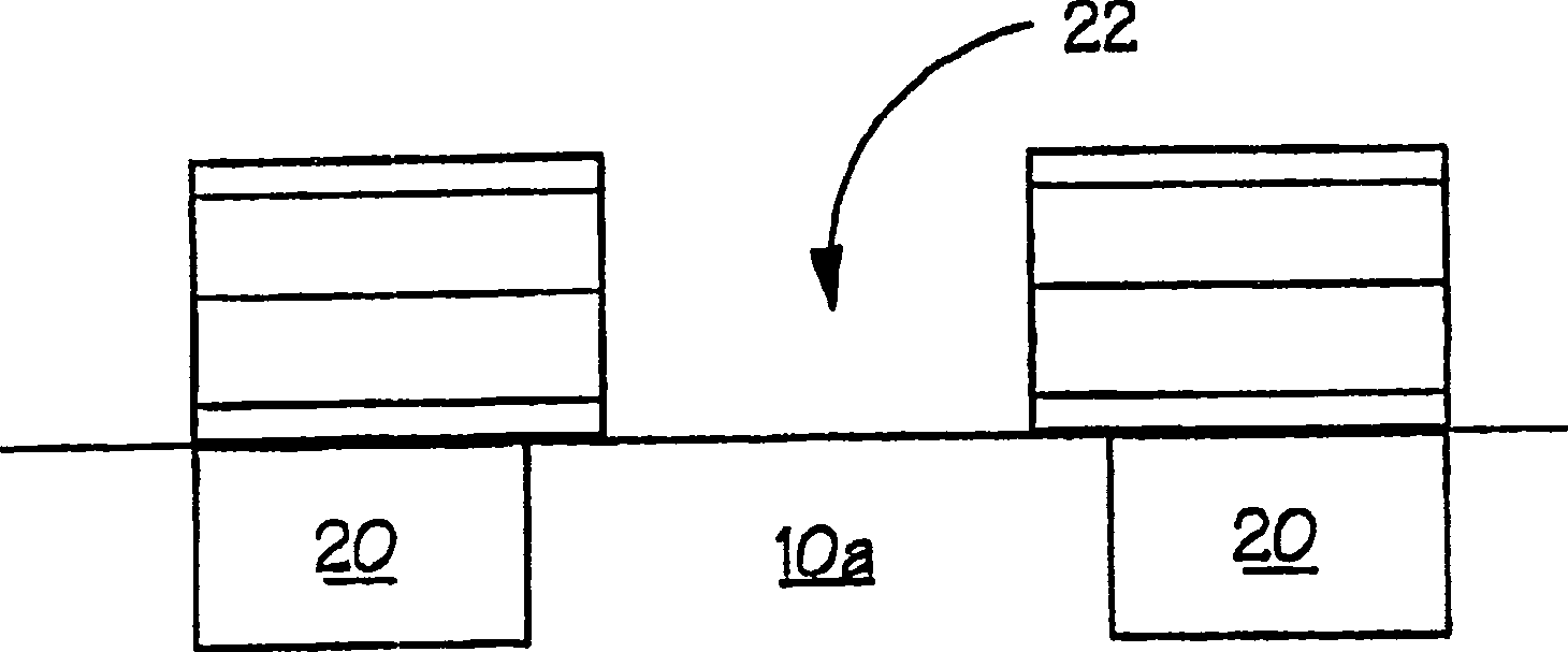
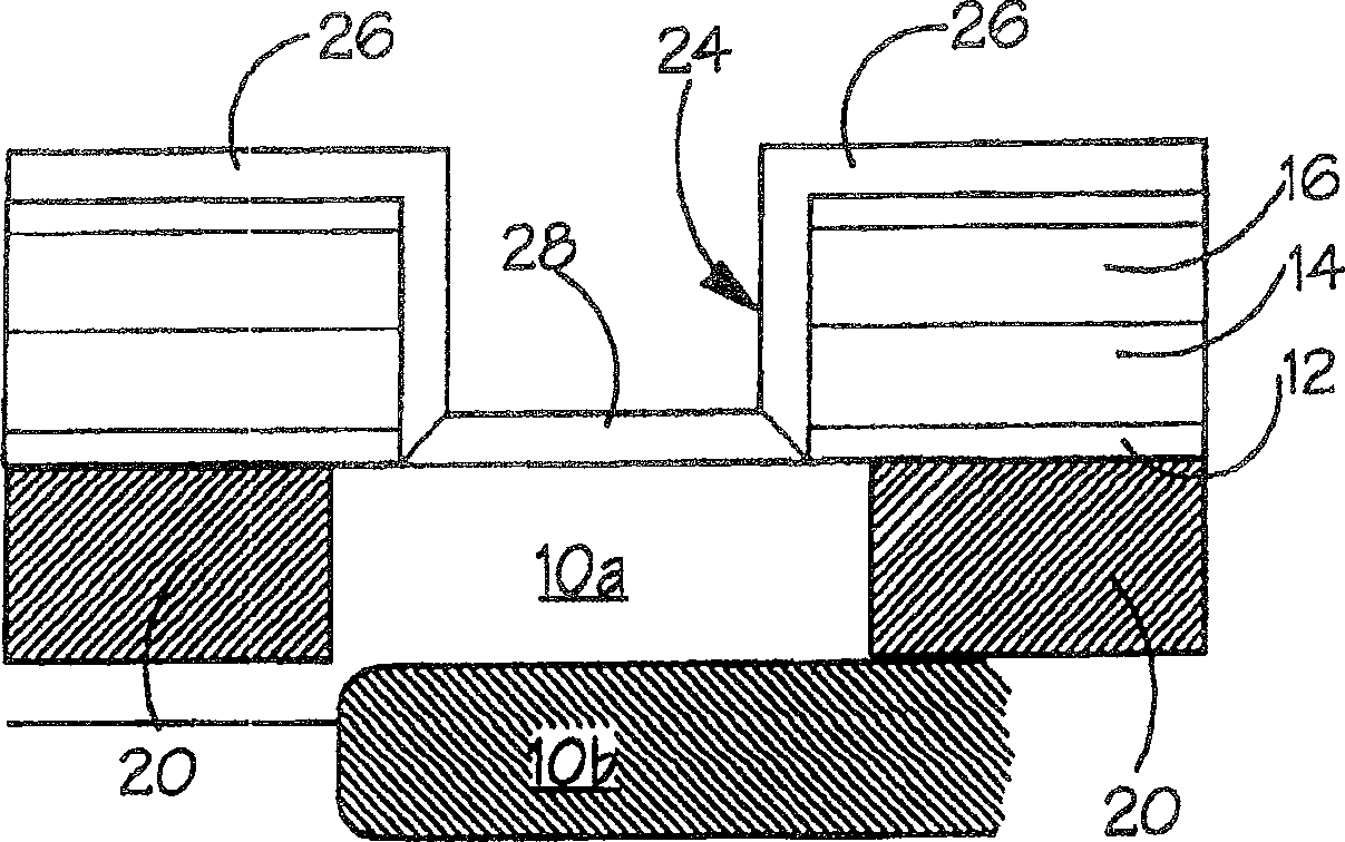
[0022] Refer below figure 2 , which is an enlarged detail of the active region, the transistor region 22 is opened by etching a well through the entire layered stack formed on the thermal oxide layer 12. This is accomplished using a plasma etch step to etch through the amorphous silicon layer 18, the TEOS layer 16, and the polysilicon layer 14. Thermal oxide 12 se...


PUM


Abstract

The invention provides a method of manufacturing a semiconductor device comprising a non-selectively grown SiGe(C) heterojunction bipolar transistor, the method comprising the steps of: forming an insulating layer (12, 40) on a substrate and forming an insulating layer (12, 40) on the insulating A layered structure comprising a conductive layer (14,42) is provided on the layer (12,40), a transistor area window (12,44) is corroded by the conductive layer (14,42), and a transistor area window (22,44) Depositing a SiGe base layer (24, 46) on the inner walls, and forming an insulator (32, 52) on the upper surface to fill the transistor area window, wherein, before the filling step, the nitride layer (30, 50) is formed as The inner layer of the transistor area window (22, 44).

Description

technical field [0001] The present invention relates to the fabrication of semiconductor devices comprising SiGe heterojunction bipolar transistors, including bipolar transistors such as SiGeC heterojunction bipolar transistors. [0002] Specifically, the present invention relates to a method for manufacturing a semiconductor device comprising a SiGe(C) heterojunction bipolar transistor by a non-selective epitaxial growth method, the method comprising the following steps: forming an insulating layer on a substrate, Providing a layer structure comprising a conductive layer on the insulating layer, etching a transistor area window through the conductive layer, depositing a SiGe base layer in the transistor area window, and including the steps of filling the transistor area window with an insulator to be etched subsequently. [0003] In this way, the present invention can relate to SiGe(C) heterojunction bipolar transistors using non-selective epitaxial growth, the intrinsic SiGe...

Claims


Application Information

Patent Timeline
Patent Type & Authority Patents(China)
IPC IPC(8): H01L21/331H01L29/732H01L29/737
CPCH01L29/66242H01L29/737
Inventor P·H·C·马格尼J·J·T·M·唐克斯
Owner NXP BV
Why Eureka
Try Eureka