

Method for making opening and contact window
A manufacturing method and dielectric layer technology, which can be used in semiconductor/solid-state device manufacturing, electrical components, circuits, etc., can solve problems such as cost increase, and achieve the effect of suppressing outgassing.
- Summary
- Abstract
- Description
- Claims
- Application Information
AI Technical Summary
Problems solved by technology
Method used
Image

Examples
no. 1 example
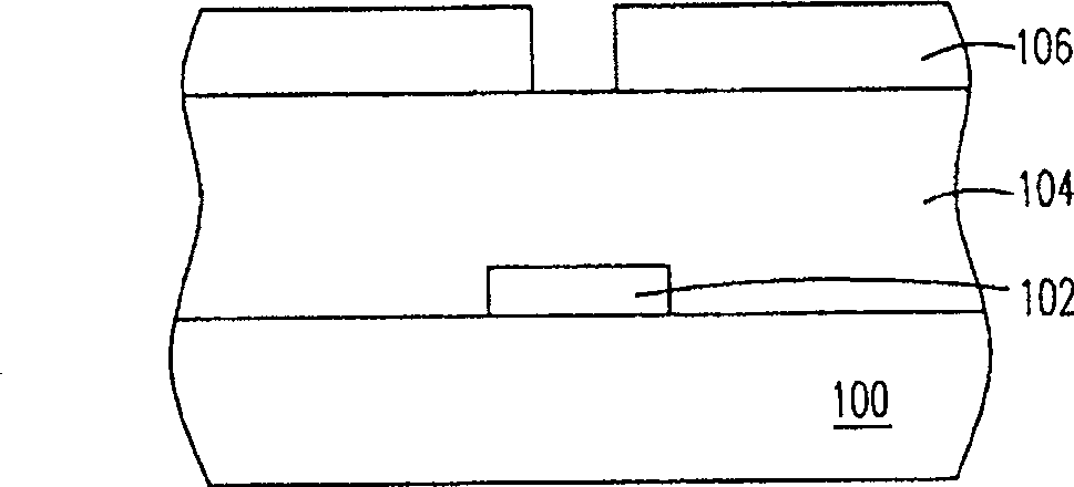
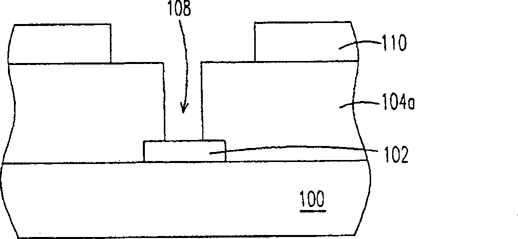
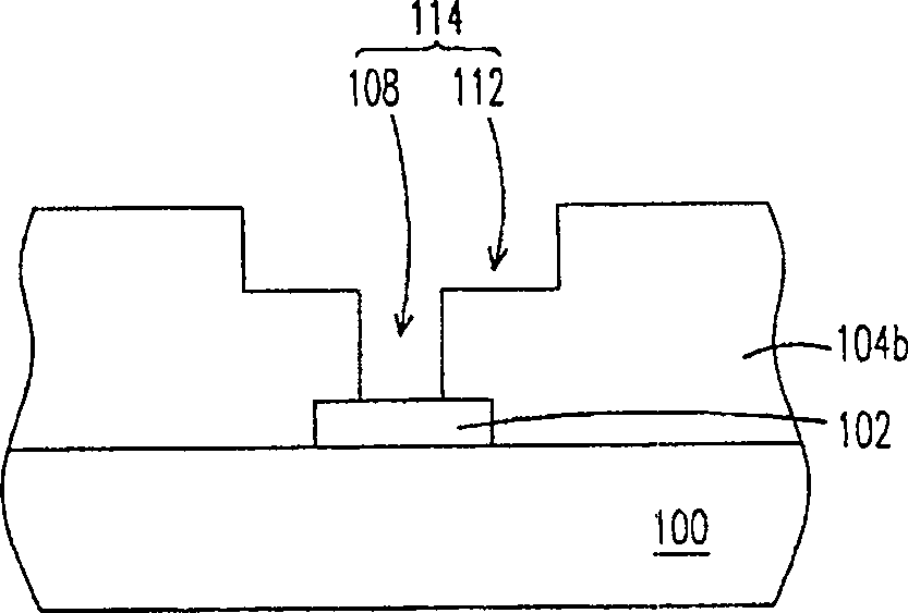
[0041] Figure 2A to Figure 2C is a cross-sectional view showing the manufacturing process of an opening according to the first preferred embodiment of the present invention.
[0042] First, please refer to Figure 2A , forming a dielectric layer 210 on a conductive layer 200 . Wherein, the material of the conductor layer 200 is, for example, copper, which is formed on a semiconductor substrate (not shown), and is used to electrically connect with other components on the substrate. The material of the dielectric layer 210 is, for example, a low dielectric constant dielectric material or fluorine-containing silicate glass, and the formation method is, for example, chemical vapor deposition. Next, a patterned mask layer 220 is formed on the dielectric layer 210, and the patterned mask layer 220 exposes a portion of the dielectric layer 210 where trenches are to be formed. The material of the patterned mask layer 220 is, for example, silicon nitride, and the formation method i...
no. 2 example
[0047] Figure 3A to Figure 3B It is a cross-sectional view showing the manufacturing process of an opening according to the second preferred embodiment of the present invention.
[0048] First, please refer to Figure 3A , forming a dielectric layer 310 with a contact window opening 314 on a conductive layer 300 , and the contact window opening 314 exposes the surface of the conductive layer 300 . Wherein, the material of the conductor layer 300 is, for example, copper, which is formed on a semiconductor substrate (not shown), and is used to electrically connect with other components on the substrate. In addition, the method of forming a dielectric layer 310 with a contact window opening 314 is, for example, to first form a dielectric material layer (not shown) by chemical vapor deposition, and its material is, for example, a low dielectric constant dielectric material or The fluorine-containing silicon glass is formed by performing a photolithography process and an etching...
no. 3 example
[0053] Figure 4A to Figure 4B It is a cross-sectional view showing the manufacturing process of an opening according to the third preferred embodiment of the present invention.
[0054] First, please refer to Figure 4A , forming a dielectric layer 410 with a trench 416 on a conductive layer 400 . Wherein, the material of the conductor layer 400 is, for example, copper, which is formed on a semiconductor substrate (not shown), and is used for electrically connecting with other components on the substrate. In addition, the method of forming a dielectric layer 410 with a trench 416, for example, is to first form a dielectric material layer (not shown) by chemical vapor deposition, the material of which is, for example, a low dielectric constant dielectric material or containing Fluorosilicate glass is formed by performing a photolithography process and an etching process.
[0055] Next, please continue to refer to Figure 4A , performing a treatment step on the exposed surf...
PUM
| Property | Measurement | Unit |
|---|---|---|
| thickness | aaaaa | aaaaa |
Abstract
Description
Claims
Application Information