Two-dimensional complete band gap photon crystal and depolarization beam splitter

A Depolarization Beamsplitter, Photonic Crystal Technology

Inactive Publication Date: 2009-09-16
HARBIN ENG UNIV
View PDF6 Cites 0 Cited by
  • Summary
  • Abstract
  • Description
  • Claims
  • Application Information

AI Technical Summary

Problems solved by technology

The depolarization beam splitter is a device that decomposes an incident unpolarized electromagnetic wave into two beams with the same light intensity ratio. At present, it is realized by using a beam splitter. The photonic crystal depolarization beam splitter has not been reported yet.

Method used


Image

  • Two-dimensional complete band gap photon crystal and depolarization beam splitter
  • Two-dimensional complete band gap photon crystal and depolarization beam splitter
  • Two-dimensional complete band gap photon crystal and depolarization beam splitter

Examples


Embodiment 1

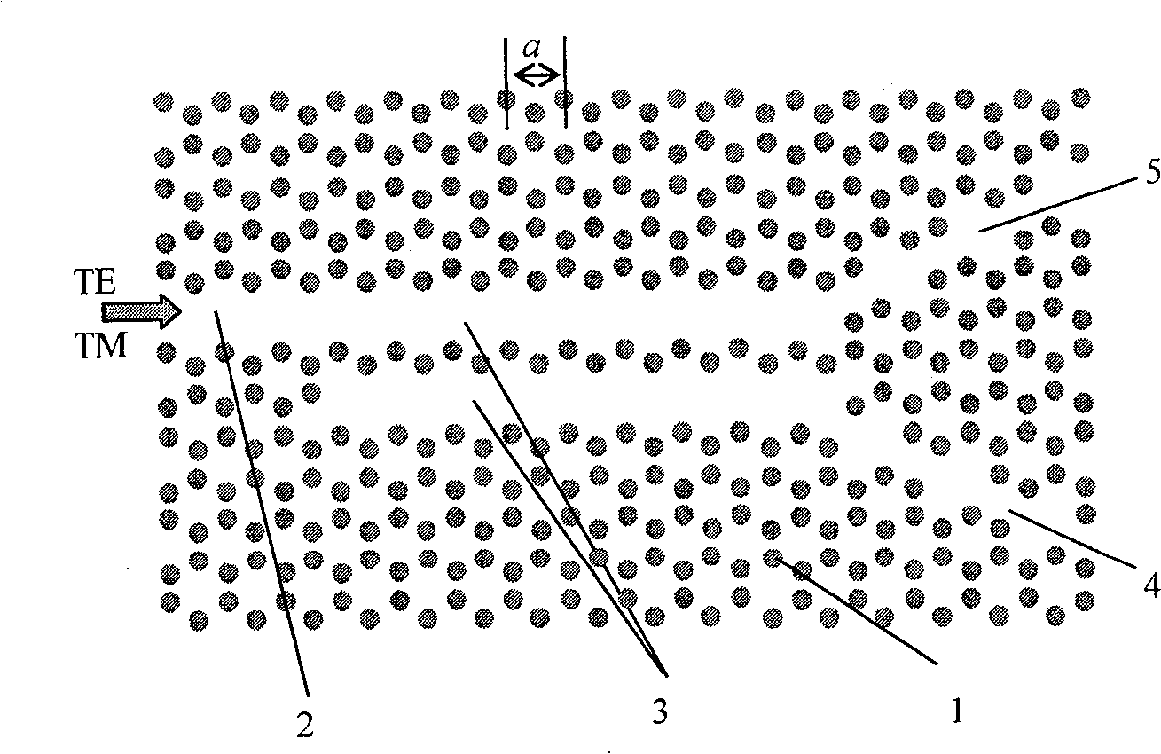
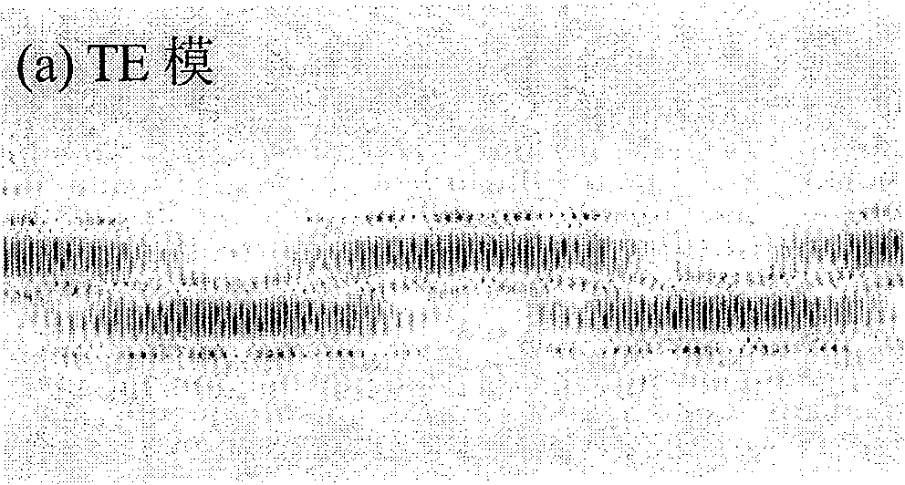
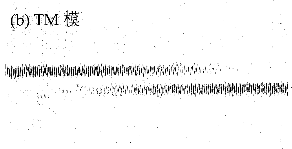
[0018] take figure 1 The hexagonal honeycomb structure is shown, the background is air, the lattice constant is a, the relative permittivity ε of the silicon Si dielectric column is 11.38, the radius of the dielectric column is about 0.15a, and the input waveguide and the output waveguide are composed of two rows of dielectric rod defects Composition, the distance between two parallel waveguides in the coupling area is 2 rows of dielectric rods. When the coupling length area is 80a, when the normalized frequency of the incident light wave ωa / 2πc=0.9743, it can be used in the polarization beam splitter, ω is the frequency of the light wave, c is the speed of light in vacuum, and the field distribution corresponding to the two modes of TE and TM As shown in Figure 2.

Embodiment 2

[0020] take figure 1 The hexagonal honeycomb structure is shown, the background is air, the lattice constant is a, the relative permittivity ε of the silicon Si dielectric column is 11.38, the radius of the dielectric column is about 0.15a, and the input waveguide and the output waveguide are composed of two rows of dielectric rod defects Composition, the distance between two parallel waveguides in the coupling area is 2 rows of dielectric rods. When the length of the coupling area is 30a, when the normalized frequency of the incident light wave is ωa / 2πc=0.9822, it can be used in the depolarization beam splitter, ω is the frequency of the light wave, c is the speed of light in vacuum, and the fields corresponding to the two modes of TE and TM The distribution is shown in Figure 3.


PUM


Abstract

The invention provides a two-dimensional complete bandgap photonic crystal depolarization beam splitter. The lattice arrangement of the photonic crystal is a hexagonal honeycomb shape, which includes an input waveguide and two output waveguides. There is a coupling area parallel to each other between the input waveguide and the output waveguide, and the output end of the coupling area is connected to the output waveguide through a bent waveguide. , both the input waveguide and the output waveguide are composed of 2 rows of dielectric rod defects, and the distance between two parallel waveguides in the coupling area is 1-3 rows of dielectric rods. The obvious advantage of the structure of the present invention is that it has a complete photon band gap, can realize both polarization beam splitting and depolarization beam splitting, and is small in size and easy to integrate.

Description

(1) Technical field [0001] The invention relates to an optical wave splitter and belongs to the field of optoelectronic technology. (2) Background technology [0002] Photonic crystal (Photonic Crystal) is a structure in which the dielectric is periodically distributed. It is characterized by the existence of a photon frequency band gap. Light with a frequency within the photon frequency band gap cannot be transmitted in the photonic crystal, but it can be arbitrarily controlled by introducing defects. The flow of light waves. Compared with traditional waveguide devices, photonic crystal functional devices have important application prospects due to their rich optical characteristics, such as using photonic crystals to make mirrors, antennas, optical switches, optical amplifiers, optical waveguides, microcavities, and thresholdless Lasers, etc.; commercialized large-core photonic crystal single-mode fiber, air hole microstructure fiber, highly nonlinear photonic crystal fib...

Claims


Application Information

Patent Timeline
Patent Type & Authority Patents(China)
IPC IPC(8): G02B6/27G02B6/26G02B6/02
Inventor 关春颖史金辉苑立波
Owner HARBIN ENG UNIV
Why Eureka
Try Eureka