
Method for detecting unwanted interface charge of mercury cadmium telluride thin film photovoltaic device

A technology of interface charge and thin-film photovoltaics, applied in the direction of measuring electric variables, instruments, measuring devices, etc., can solve problems such as unimportant, limiting the effect of C-V method, unable to extract interface charge information, etc., and achieve the effect of non-damage judgment

Inactive Publication Date: 2009-11-11
SHANGHAI INST OF TECHNICAL PHYSICS - CHINESE ACAD OF SCI
View PDF2 Cites 0 Cited by
  • Summary
  • Abstract
  • Description
  • Claims
  • Application Information

AI Technical Summary

Problems solved by technology

This method gives the comprehensive information of the interface charge, but cannot independently give the information of the interface charge that affects the photoelectric response of the device. For photovoltaic detectors, people are most concerned about the impact on the photoelectric response of the device. The effective interface charge of , that is, the harmful interface charge, and the non-harmful interface charge can be ignored for the time being, because the non-harmful interface charge that has no effect on the photoelectric response of the device is not important for optimizing the device performance
Because the traditional electrical C-V method cannot extract the interface charge information related to the photoelectric response of the device, which greatly limits the role of the C-V method in actual measurement. Therefore, people expect a more effective method to obtain interface charge information

Method used


Image

  • Method for detecting unwanted interface charge of mercury cadmium telluride thin film photovoltaic device
  • Method for detecting unwanted interface charge of mercury cadmium telluride thin film photovoltaic device
  • Method for detecting unwanted interface charge of mercury cadmium telluride thin film photovoltaic device

Examples


Embodiment Construction

[0017] Below in Hg 0.702 CD 0.298 Te thin-film photovoltaic device is an embodiment in conjunction with the accompanying drawings to describe in detail the specific implementation of the present invention:

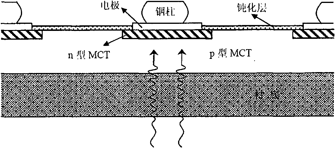
[0018] The measured sample is a planar junction HgCdTe linear photovoltaic detector grown by molecular beam epitaxy, see figure 1 . p-Hg 0.702 CD 0.298 Te grows on the CdTe buffer layer with GaAs substrate. Boron ions are implanted on the p-type surface to form n + type mutation n + -p knot. Samples were flip-bonded on sapphire substrates.

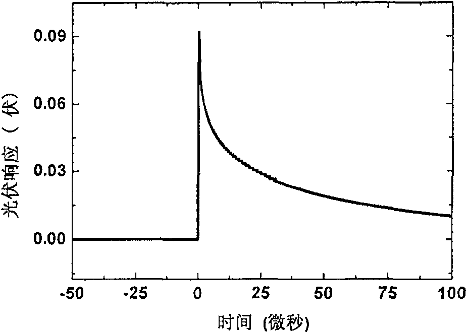
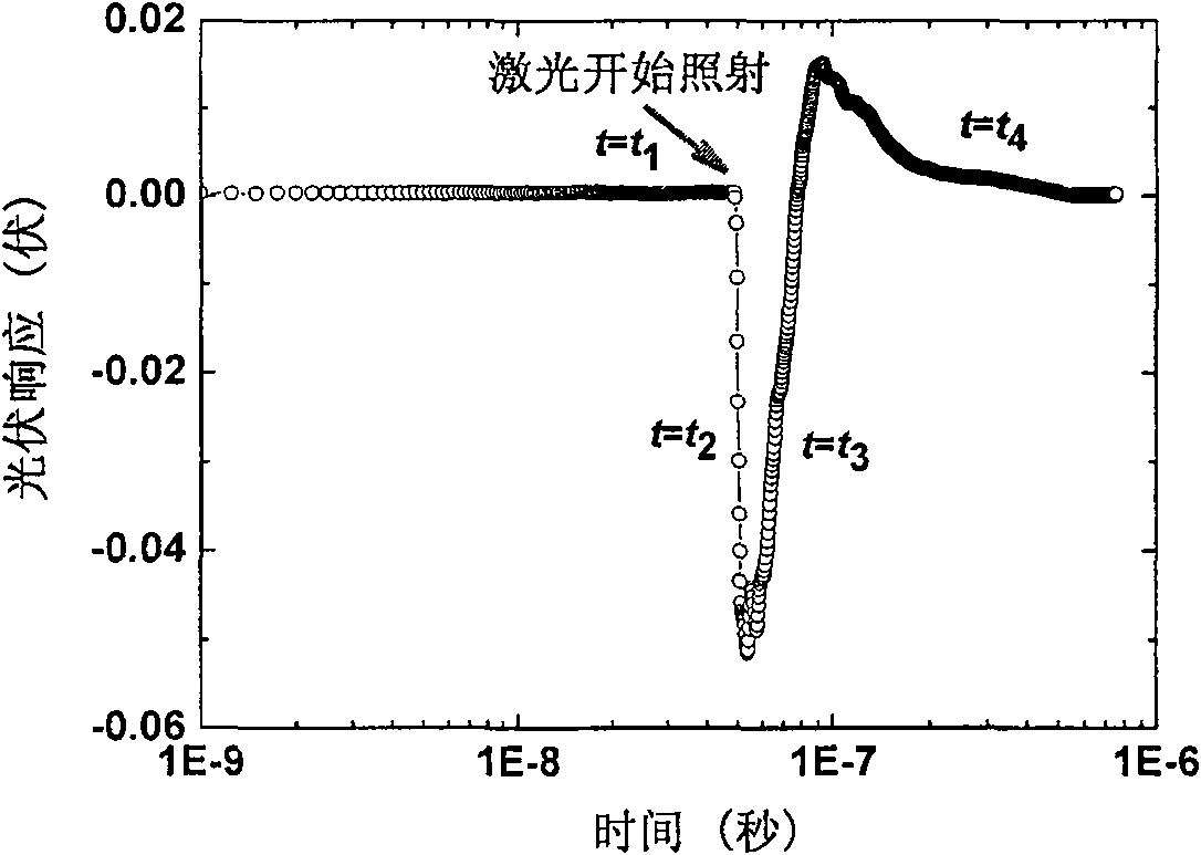
[0019] The tunable pulse laser is pumped by PL2143BSS Nd:YAG laser produced by Lithuania EKSPLA company to pump PG401 / DFG optical parameter generator / difference frequency amplifier. The laser pulse width is 30ps, repetition frequency is 10Hz, and its output wavelength is adjusted to 4.5μm. Calculated, Hg at 4.5μm incident wavelength 0.702 CD 0.298 The absorption coefficient of Te is α 4.5μm =4870cm -1 , Hg 0.702 CD 0.29...


PUM


Abstract

The invention discloses a method for detecting harmful interface charges of mercury cadmium telluride thin-film photovoltaic devices. The method uses a beam of ultrafast pulsed laser light with photon energy greater than the band gap of the tested device to back-irradiate the HgCdTe device, and uses a digital oscilloscope to measure the two phases of the photovoltaic device. The evolution relationship between the transient photovoltaic signal between electrodes and time, according to the interface charge-induced electric field measured by the external circuit and the photo-generated electromotive force formed by the pn junction electric field are separated in the time dimension, and the photo-generated electromotive force formed by the interface charge-induced electric field and the effective The identification of the photoelectromotive force formed by the built-in electric field of the metallurgical pn junction can easily obtain the information of the interface charge that has a great influence on the photoelectric response of the device. This is a convenient, rapid and non-destructive identification method, which is of great significance for improving device performance, improving device stability, and guiding people to explore new devices.

Description

technical field [0001] The invention relates to performance measurement of mercury cadmium telluride (HgCdTe) thin-film photovoltaic devices, in particular to a method for measuring harmful charges on the HgCdTe / CdTe interface of the HgCdTe thin-film photovoltaic device. Background technique [0002] Hg 1-x CD x Te is an important material for the preparation of medium-wave (3-5 μm) and long-wave (8-14 μm) infrared focal plane devices, and is widely used in military, aerospace and other fields. Although the preparation technology of mercury cadmium telluride materials is becoming more and more mature, a considerable amount of fixed interface charges still inevitably appear when growing mercury cadmium telluride on the CdTe buffer layer with GaAs substrate, and its density is closely related to the process. The charge density is difficult to control, and can be positive or negative, and its density value cannot be accurately known under normal circumstances. Since HgCdTe i...

Claims


Application Information

Patent Timeline
Patent Type & Authority Patents(China)
IPC IPC(8): G01R29/24
Inventor 陆卫崔昊杨李志锋李宁甄红楼张波陈平平李天信陈效双胡伟达叶振华胡晓宁
Owner SHANGHAI INST OF TECHNICAL PHYSICS - CHINESE ACAD OF SCI
Learn More