Semiconductor package substrate for improving deform

A technology for packaging substrates and semiconductors, applied in semiconductor devices, semiconductor/solid-state device parts, electric solid-state devices, etc., to achieve the effects of avoiding deformation, reducing the degree of subsidence and collapse, and preventing wrinkles or deformation

Active Publication Date: 2010-01-13
CHIPMOS TECH INC
View PDF2 Cites 1 Cited by
  • Summary
  • Abstract
  • Description
  • Claims
  • Application Information

AI Technical Summary

Problems solved by technology

[0007] The main purpose of the present invention is to provide a semiconductor packaging substrate with improved deformation, which can prevent the flexible dielectric layer from wrinkling or deforming by using a mesh or other special-shaped reinforcing metal pattern formed in the blank area of ​​the lead. Problem, it has the effect of uniform distribution of stress, provides better toughness and barrier function, especially can reduce the deformation such as subsidence and collapse in the section from the two transmission sides to the center of the substrate

Method used


Image

  • Semiconductor package substrate for improving deform
  • Semiconductor package substrate for improving deform
  • Semiconductor package substrate for improving deform

Examples


no. 1 Embodiment

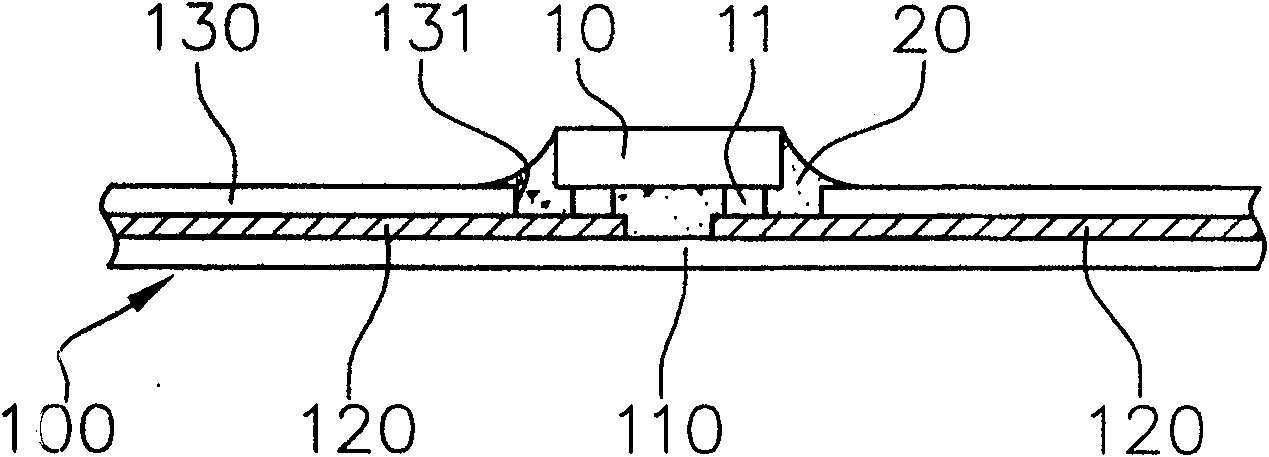
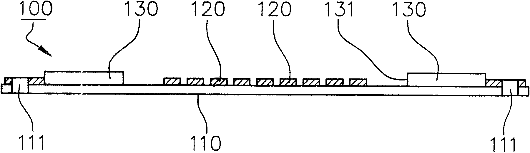
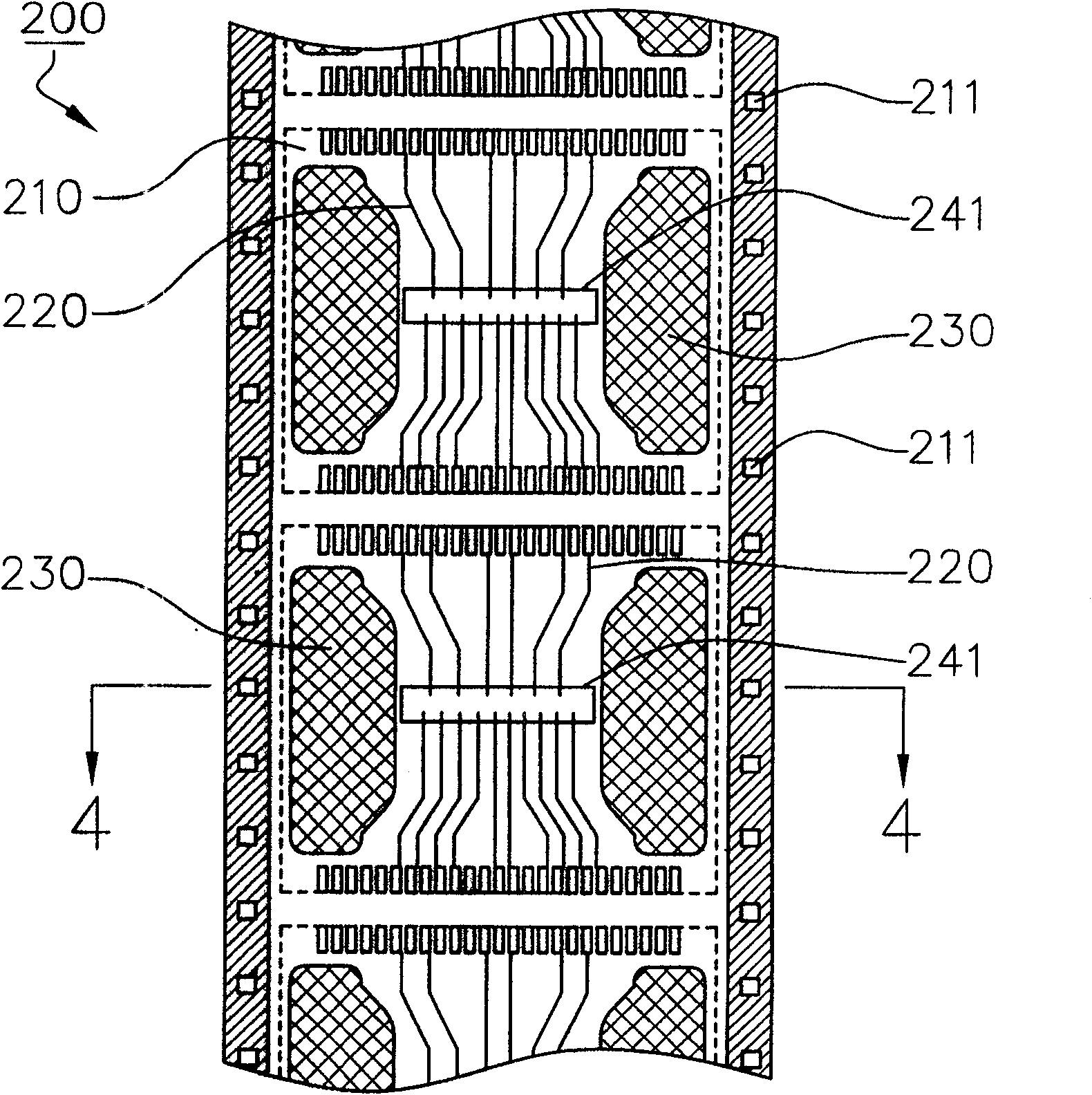
[0046] According to a first embodiment of the present invention, a semiconductor packaging substrate with improved deformation is disclosed. Such as image 3 and Figure 4 As shown, the semiconductor package substrate 200 mainly includes a flexible dielectric layer 210 , a plurality of pins 220 , at least one reinforcing metal pattern 230 and a solder resist layer 240 . The pins 220 and the reinforcing metal pattern 230 are formed on the same surface of the flexible dielectric layer 210 . The flexible dielectric layer 210 is an organic dielectric film layer, and usually the material of the flexible dielectric layer 210 can be polyimide (polyimide, PI) or polyester (PET), etc., as these lead The carrier film of the feet 220 and the reinforcing metal pattern 230 is particularly suitable for tape-and-roll transport for semiconductor packaging operations. The semiconductor package substrate 200 includes a plurality of carrier units corresponding to packaged products.

[0047]T...


PUM


Abstract

A semiconductor package substrate for preventing deformation mainly comprises a flexible dielectric layer, a plurality of pins, at least one reinforced metal pattern and a solder mask layer. All the pins and the reinforced metal pattern are formed on the same surface of the flexible dielectric layer, and the reinforced metal patterns are used for filling the pin blank section of the flexible dielectric layer. The solder mask layer is formed on the flexible dielectric layer to locally cover the pins and to cover or expose the reinforced metal patterns according to different application. The net-shaped formation positions of the reinforced metal patterns can prevent the flexible dielectric layer from crinkling or deforming.

Description

technical field [0001] The invention relates to a semiconductor packaging carrier, in particular to a semiconductor packaging substrate with improved deformation. Background technique [0002] Existing semiconductor packaging substrates can be used to carry chips in semiconductor packaging operations. The semiconductor packaging substrates should have the characteristics of electrical interconnection, high temperature resistance, and deformation resistance for carrying chips. In semiconductor packaging operations, both chip bonding and encapsulant curing will cause the substrate to be in a high temperature state. Chip bonding requires a higher temperature but a short time, and encapsulant curing requires a lower temperature but a longer time. Especially for flexible / soft substrates, due to the long-term heating in the oven and the weight of the wafer, the section from the two transmission sides of the substrate to the wafer side is prone to deformation, sinking and collapse,...

Claims


Application Information

Patent Timeline
Patent Type & Authority Patents(China)
IPC IPC(8): H01L23/498H05K1/02
CPCH01L2224/73204H01L2224/16225
Inventor 李明勋洪宗利
Owner CHIPMOS TECH INC
Why Eureka
Try Eureka