Manufacturing method and structure of metal interconnector

A technology of interconnection and metal, applied in semiconductor/solid-state device manufacturing, electrical components, electric solid-state devices, etc., can solve the problems of insufficient shielding, unusability, phase change, etc., and achieve the effect of avoiding phase change

Active Publication Date: 2007-07-18
UNITED MICROELECTRONICS CORP
View PDF0 Cites 23 Cited by
  • Summary
  • Abstract
  • Description
  • Claims
  • Application Information

AI Technical Summary

Problems solved by technology

However, a photoresist layer that is too thin will cause problems such as insufficient shielding and boundary defects in the etching process, so the etching process cannot only use the photoresist layer pattern as an etching mask, but must use a hard mask craft
However, the 45nm process cannot use the commonly used polysilicon hard mask, because it will cause phase changes in metal silicides such as nickel silicide on the surface of the device.
[0008] In addition, the above-mentioned prior art still has a disadvantage when making metal interconnections, that is, it is necessary to deposit an etch stop layer before forming trenches. If the hard mask process proposed by the present invention is used, the process of depositing an etch stop layer can be omitted. one step

Method used


Image

  • Manufacturing method and structure of metal interconnector
  • Manufacturing method and structure of metal interconnector
  • Manufacturing method and structure of metal interconnector

Examples


Embodiment Construction

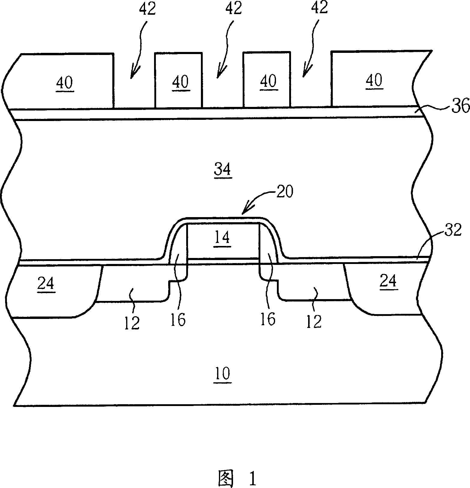
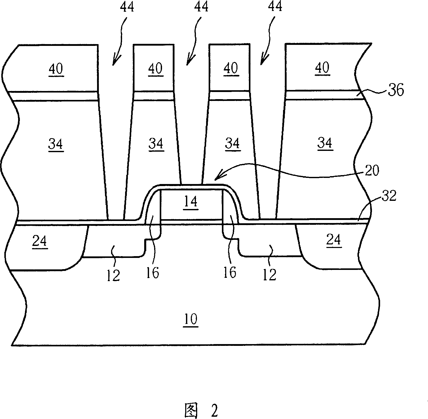
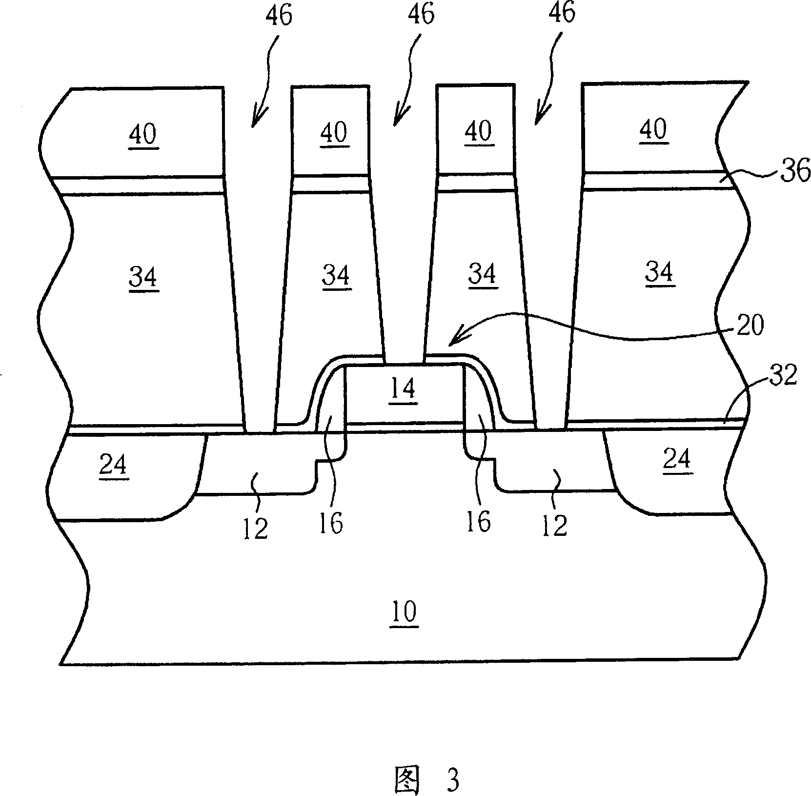
[0041]Please refer to Figure 12 to Figure 20. 12 to 20 are schematic diagrams of a method for fabricating a metal interconnection according to a preferred embodiment of the present invention. As shown in Figure 12, at first a semiconductor substrate 62 is provided, such as a semiconductor wafer (wafer) or a silicon-on-insulator substrate (SOI), etc., and at least one MOS transistor element 72 is formed on the semiconductor substrate 62, which includes The source / drain region 64 is disposed in the semiconductor substrate 62 , a gate structure 66 is disposed on the semiconductor substrate 62 , and a spacer 68 is disposed on a surrounding wall of the gate structure 66 . At the same time, the surface of the gate structure 66 and the source / drain region 64 of the MOS transistor element 72 also includes a layer of metal silicide (silicide) 70, and its material can be silicide formed by a self-aligned metal silicide process (salicide). Nickel (NiSi), etc., and the MOS transistor ele...


PUM


Abstract

The invention relates to an inter-wire technology in metal and its structure, which provides a substrate with the first conductor. Firstly, it forms the first dielectric layer and the first pattern hard mask on the substrate. Then it etches the first hard mask to form the first shedding and the second conductor, and forms the second dielectric layer and the second hard mask on the firs hard mask. Finally, it takes the second hard mask as the etching mask and takes the first hard mask as the etching stop layer to form the second shedding and the third conductor.

Description

technical field [0001] The invention relates to a metal interconnection process and structure, in particular to a metal interconnection process and structure using a hard mask as an etching mask and an etching stop layer. Background technique [0002] As the line width of integrated circuits continues to shrink, the miniaturization of semiconductor elements has entered the nanometer level, and the integration of a single chip, that is, the greater the density of semiconductor elements on it, means the smaller the spacing between elements. This makes the manufacture of contact holes and metal interconnections more and more difficult. [0003] Please refer to Figure 1 to Figure 11. 1 to 11 are schematic diagrams of methods for manufacturing contact holes and metal interconnections in the prior art. As shown in FIG. 1, a semiconductor substrate 10 is first provided, and at least one metal-oxide-semiconductor (MOS) transistor element 20 is formed on the semiconductor substrate...

Claims


Application Information

Patent Timeline
Patent Type & Authority Applications(China)
IPC IPC(8): H01L21/768H01L23/522
Inventor 周珮玉黄俊仁
Owner UNITED MICROELECTRONICS CORP
Why Eureka
Try Eureka