Wafer-level encapsulation and cutting method

A technology of wafer-level packaging and cutting method, which is applied in the manufacturing of electrical components, electric solid-state devices, semiconductor/solid-state devices, etc., and can solve the problems of structural damage, decline in yield, and large package die size.

Inactive Publication Date: 2007-08-01
TOUCH MICRO SYST TECH
View PDF0 Cites 19 Cited by
  • Summary
  • Abstract
  • Description
  • Claims
  • Application Information

AI Technical Summary

Problems solved by technology

The size of the packaged die produced by this packaging method is slightly larger, and the packaging process is cumbersome, which does not meet the current requirements of electronic products that emphasize thinness and small size, and is not suitable for mass production; moreover, the bottleneck of this packaging technology often appears In the later cutting process, external mechanical force may cause structural damage, and the particles generated during the cutting process may contaminate the product, resulting in a decrease in yield

Method used


Image

  • Wafer-level encapsulation and cutting method
  • Wafer-level encapsulation and cutting method
  • Wafer-level encapsulation and cutting method

Examples


Embodiment Construction

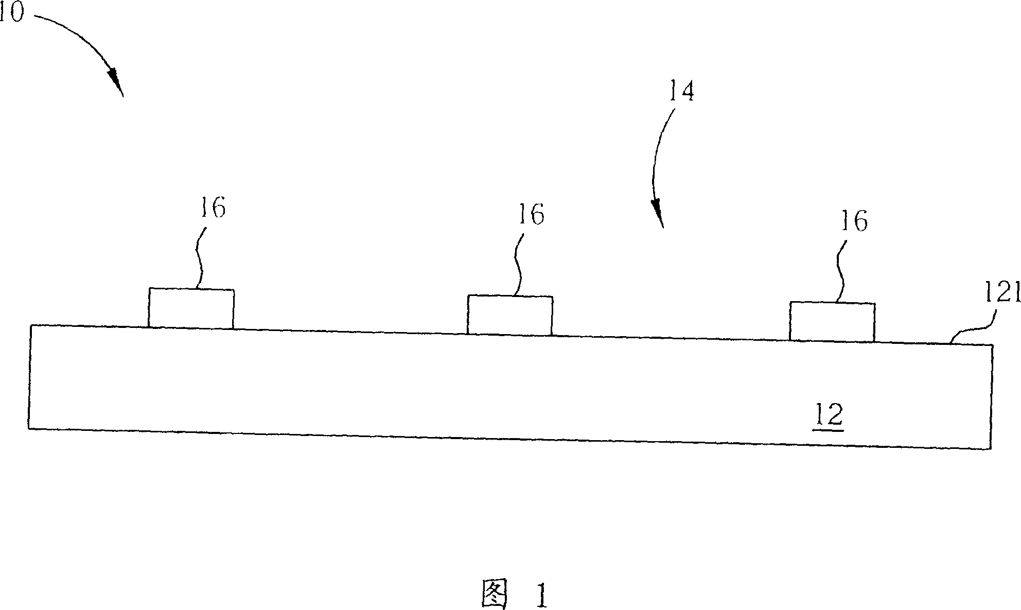
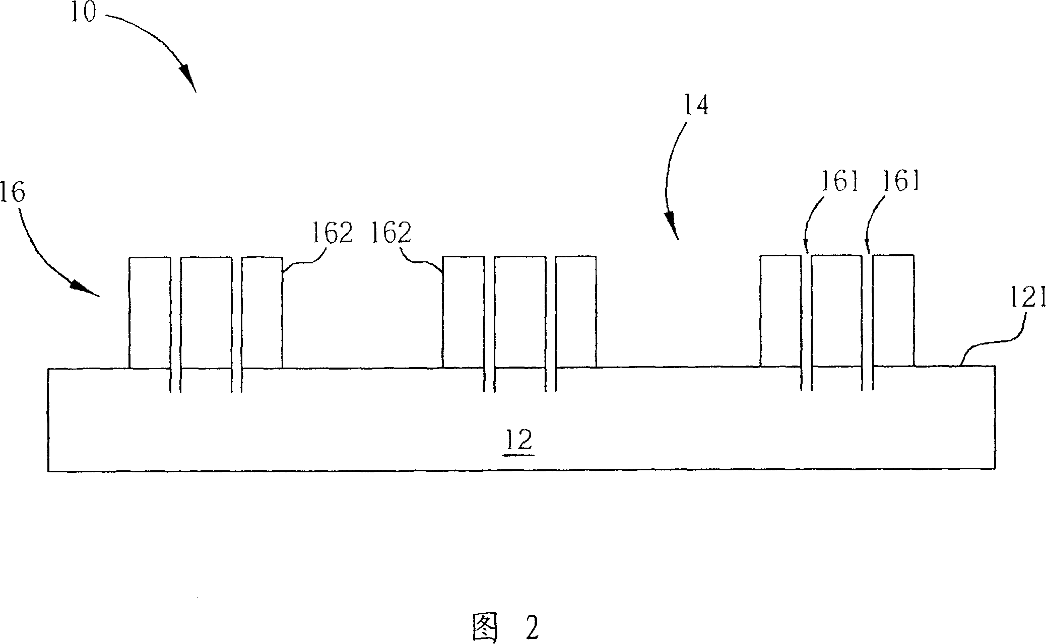
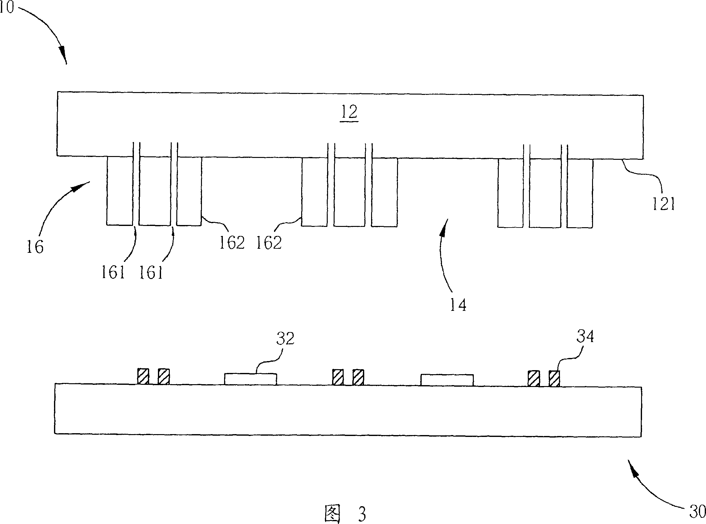
[0018] 1 to 9 are schematic diagrams of a wafer-level packaging cutting method according to a preferred embodiment of the present invention. As shown in FIG. 1, FIG. 1 is a packaging chip 10 used as an upper cover structure. The packaging chip 10 includes a transparent substrate 12, a wafer pattern 16 and a plurality of concave cavities 14 defined by the wafer pattern 16, and the cavity 14 is located on the front side 121 of the packaging chip 10 . The transparent substrate 12 is made of quartz, plastic or glass or other transparent materials, and in this embodiment, the transparent substrate 12 is a glass substrate. Referring to FIG. 2 , the packaged wafer 10 is subjected to a pre-cutting process according to a predetermined position, wherein the pre-cutting process can be wet wafer dicing, such as a wet etching process, or dry wafer dicing, such as a dry etching process or using a dicing tool. The above-mentioned pre-cutting process forms a plurality of grooves 161 on the w...


PUM


Abstract

Firstly encapsulated wafer and component wafere are provided, and the frontispiece of the encapsulated wafer possesses many cavities and grooves. Then the encapsulated wafer and component wafere are jointed, and the first incising craft is preceded. Then the adhesion layer is adhibited to the encapsulated wafer, the second incising craft is preceded and the adhesion layer is removed to form the wafer-class encapsulation structure. At last, the wafer-class encapsulation structure is incised into several encapsulated cores.

Description

technical field [0001] The invention relates to a packaging and cutting method, in particular to a wafer-level packaging and cutting method. Background technique [0002] The packaging of semiconductor components is an important step in its process. The so-called packaging refers to the combination of the core structures in the device. The function of packaging is to protect fragile semiconductor components (such as optical components, micro-electromechanical components, etc.) In the case of environmental damage (such as mechanical damage or particle pollution, etc.), it also takes on the functions of mechanical support and signal output or input. [0003] The known packaging process is as follows: first, the processed wafer is cut and separated into individual dies, and the separated dies are placed on the lead frame and fixed with epoxy. This step is called die bonding, and then through steps such as wire bonding or flip-chip, the aforementioned die packaging is completed...

Claims


Application Information

Patent Timeline
Patent Type & Authority Applications(China)
IPC IPC(8): H01L21/50
CPCH01L2924/16235
Inventor 王顺达
Owner TOUCH MICRO SYST TECH
Why Eureka
Try Eureka