Metal-semiconductor field effect transistor with source-drain double-concave structure

A field effect transistor, metal semiconductor technology, applied in the field of metal semiconductor field effect transistors, can solve the problems of limited application, low critical breakdown electric field and thermal conductivity, etc., to improve frequency characteristics, good frequency characteristics and output power density, Effect of suppressing short channel effect

Inactive Publication Date: 2007-08-22
UNIV OF ELECTRONICS SCI & TECH OF CHINA
View PDF0 Cites 21 Cited by
  • Summary
  • Abstract
  • Description
  • Claims
  • Application Information

AI Technical Summary

Problems solved by technology

[0003] High-frequency MESFETs mainly use III-V compound semiconductor materials, such as gallium arsenide (GaAs), but their relatively low critical breakdown electric field and thermal conductivity limit their application in high-power fields

Method used


Image

  • Metal-semiconductor field effect transistor with source-drain double-concave structure
  • Metal-semiconductor field effect transistor with source-drain double-concave structure
  • Metal-semiconductor field effect transistor with source-drain double-concave structure

Examples


Embodiment Construction

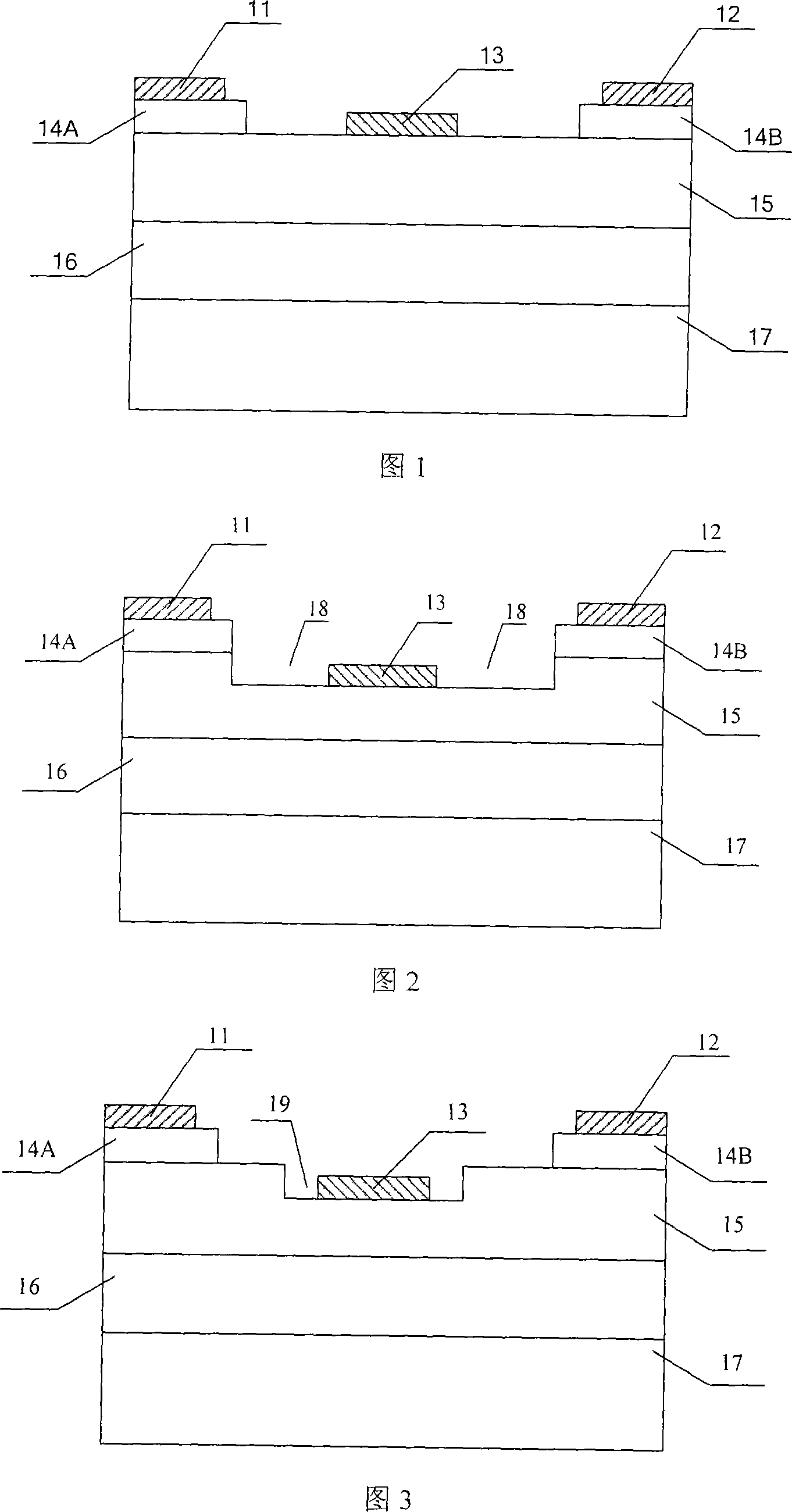
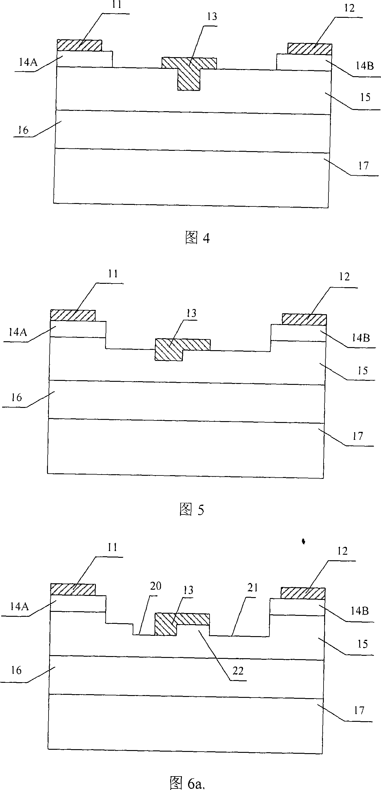
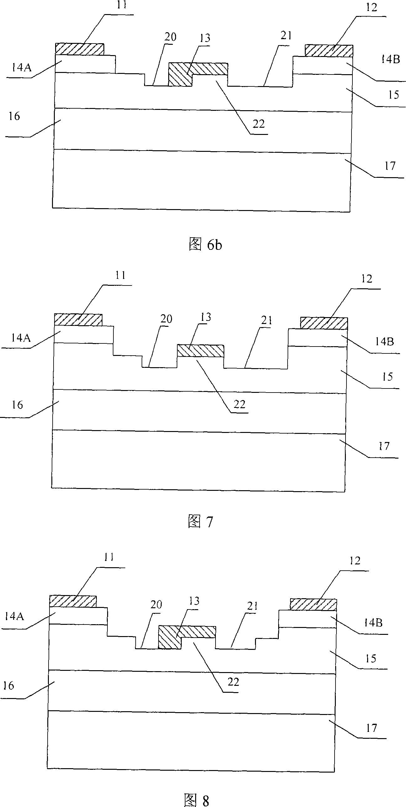
[0029] The source-drain double concave structure MESFET, as shown in Figure 6-a and Figure 6-b, includes: semi-insulating substrate 17; buffer layer 16; active layer 15; cap layers 14A and 14B; source electrode 11; drain electrode 12 ; and a gate electrode 13 in Schottky contact with the active layer. Two mutually independent grooves 20, 21 are formed by etching between the gate-drain region and between the gate-source region of the active layer 15, and a raised platform 22 is formed between the two grooves. The gate electrode can be deposited entirely on the platform; it can also be deposited in the groove between the platform and the gate-source to form a stepped structure.

[0030]Figure 6-a shows the use of a source-drain double-cavity structure on a conventional groove structure; Figure 6-b shows the use of a source-drain double-cavity structure on a conventional planar structure. Here, the structure shown in FIG. 6-a is taken as an example, and the structure of the gate...


PUM


Abstract

This invention puts forward a MESFFT structure used in HF and large power field, namely, a biconcave structure of MESFET, in which, two independent grooves are formed on the active layer between a gate source and a drain by etching and a projected platform is formed between the two grooves, the gate electrode can deposit on the platform totally or the groove between the platform and the gate source to form a step structure, and the groove between the gate source and the drain stops the exhaust layer under the gate electrode to expand to the source and drain shift region so as to reduce the source and drain capacitance to increase the frequency property of the devices, and the groove can reduce thickness of channels of the shift region and modulate the field distribution of the shift region.

Description

technical field [0001] The present invention relates to metal-semiconductor field-effect transistors, more specifically, to high-frequency, high-power metal-semiconductor field-effect transistors (Metal-Semiconductor-Field-Effect-Transistor, MESFET). Background technique [0002] In recent years, with the rapid development of microelectronics technology and the urgent needs of aerospace, electronic countermeasures and radar communications and other related fields, the development of new high-frequency and high-power semiconductor devices has attracted more and more attention. Bipolar-Junction-Transistor (BJT) and power metal-oxide-semiconductor field-effect transistor (Metal-Oxide-Semiconductor-Field-Effect-Transistor, MOSFET) have been widely used in high-power applications. BJTs are minority carrier devices and their power handling capability is limited at higher operating frequencies. Compared with MESFET, MOSFET has larger gate capacitance, which affects its frequency c...

Claims


Application Information

Patent Timeline
Patent Type & Authority Applications(China)
IPC IPC(8): H01L29/772
Inventor 张金平张波邓小川陈壮梁叶毅罗小蓉李肇基
Owner UNIV OF ELECTRONICS SCI & TECH OF CHINA
Why Eureka
Try Eureka