Surface-reinforced infrared spectrum optical device

A technology of infrared spectroscopy and optical devices, applied in the field of infrared spectroscopy, can solve the problems of metal film shedding, metal film electrochemical response deviation, and inability to give infrared signals, etc., and achieve the effect of simple and stable structure

Inactive Publication Date: 2007-09-05
FUDAN UNIV
View PDF0 Cites 8 Cited by
  • Summary
  • Abstract
  • Description
  • Claims
  • Application Information

AI Technical Summary

Problems solved by technology

Silicon column at 1000cm -1 There are strong absorption signals below, and the corresponding infrared signals cannot be given; germanium and zinc selenide are at 1000cm -1 The following absorption is weak, but the metal films on the surface of these two substrates are prepared by vacuum dry method. What is more serious is that the germanium and zinc selenide substrates are unstable in acidic solutions, which will easily cause the metal film to fall off during use, and its The electrochemical response of the upper metal film often deviates from the characteristics of the bulk metal electrode, which is not suitable for in-situ spectroelectrochemical research
Adzic group [6] The concept of combining zinc selenide cylinders and silicon wafer infrared windows was proposed, but the relevant parameters were not given. According to the knowledge of physical optics, this combination must have high requirements for the smoothness of the interface. In fact, it is very difficult in spectroelectrochemical experiments. Difficult-to-implement device design concepts

Method used


Image

  • Surface-reinforced infrared spectrum optical device
  • Surface-reinforced infrared spectrum optical device
  • Surface-reinforced infrared spectrum optical device

Examples


Embodiment Construction

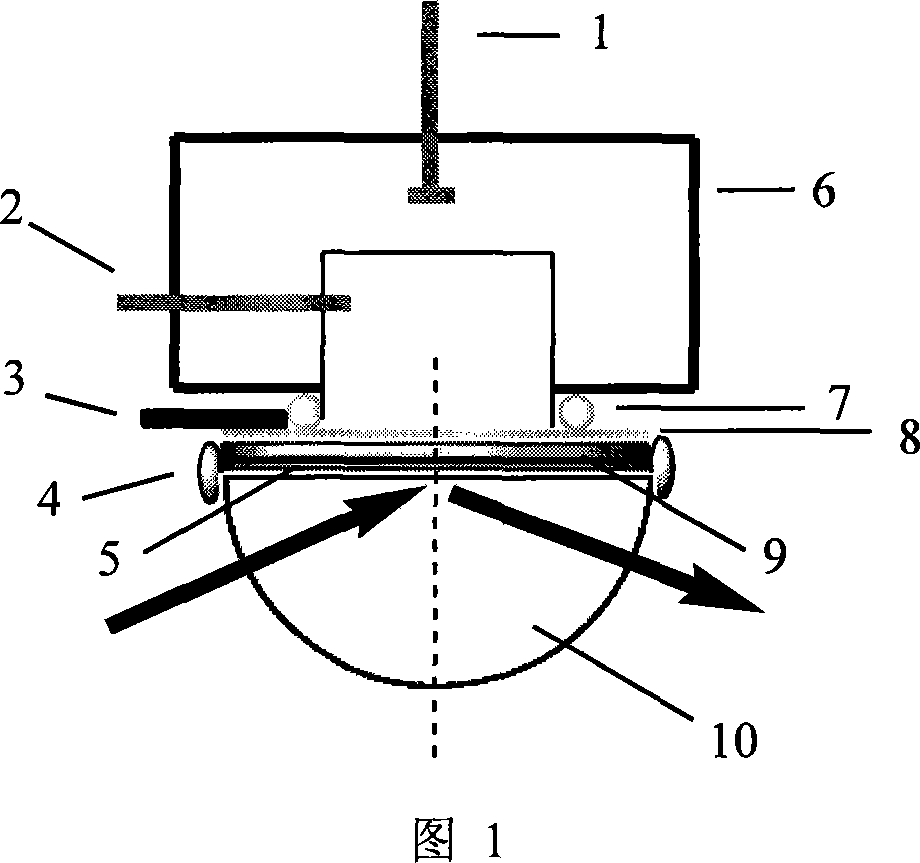
[0025] The specific structure of the device is mainly composed of an electrolytic cell, a reference electrode, a counter electrode, a metal nano-film electrode, a silicon wafer and a zinc selenide half cylinder. The size of the silicon wafer is 20mm×25mm, and the thickness is 50-200 microns; the diameter of the zinc selenide half cylinder is 20mm, and the height is 25mm. Concrete use steps are as follows: 1. at first on the surface of silicon chip 9 plate metal nano-film 8, then the silicon rubber ring 7 that diameter is 8-14mm is covered on the surface of metal nano-film, and pack in the electrolytic cell 6, then in Add the water layer to the other side of the silicon wafer 9 and squeeze the water layer with the zinc selenide half cylinder 10, and finally seal the water film 5 in the gaps around the interface with paraffin 4, which constitutes the working electrode. ② Insert the reference electrode 2 and the counter electrode 1 into the electrolytic cell, which forms a three-...


PUM

PropertyMeasurementUnit
thicknessaaaaaaaaaa
thicknessaaaaaaaaaa
diameteraaaaaaaaaa

Abstract

An infrared spectrum optical device of surface intensification type is prepared as plating metal nanofilm electrode on top surface of wafer and setting water membrane layer between bottom-side surface of water and semi-cylindrical zinc selenide as well as using paraffin wax to seal peripheral seam of water membrane layer to from operation electrode, arranging electrolyzer on metal nanofilm and sealing intermediate by silicon rubber ring, using wire copper membrane to lead out metal nanofilm and setting pair electrode and reference electrode in electrolyzer to from electrode system of electrochemical spectrum test.

Description

technical field [0001] The invention belongs to the technical field of infrared spectroscopy, and specifically relates to a surface-enhanced infrared spectroscopy optical device, which can be used in the research and application of electrochemical on-site and off-site surface-enhanced infrared spectroscopy, and can lower the lower limit of the signal interval from the usual 1000cm -1 Wavenumber extended to 700cm -1 at the wave number. Background technique [0002] Surface Enhanced Infrared Spectroscopy (SEIRAS) [1] It is an important analysis tool for studying the molecular structure information of the electrode interface. Surface-enhanced infrared absorption spectroscopy (ATR-SEIRAS) with attenuated total reflection (ATR) mode has strong surface signal and simple surface selection law, which can avoid the problems faced by traditional external reflection infrared absorption spectroscopy (IRAS), such as insufficient surface signal , Uneven electric field distribution, mas...

Claims


Application Information

Patent Timeline
Patent Type & Authority Applications(China)
IPC IPC(8): G01N21/35G01N21/25G01N21/3563
Inventor 蔡文斌薛晓康严彦刚王金意
Owner FUDAN UNIV
Why Eureka
Try Eureka